Performance Analysis of Parallel Prefix Adder Based on FPGA 6
advertisement
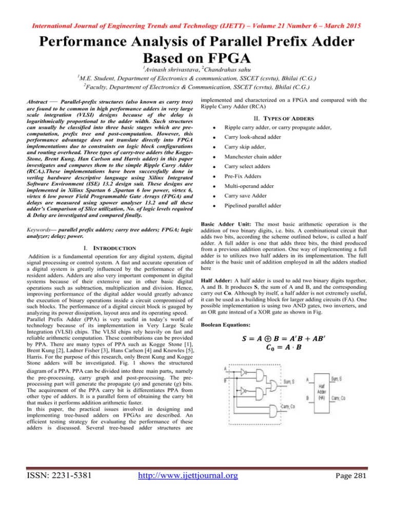
International Journal of Engineering Trends and Technology (IJETT) – Volume 21 Number 6 – March 2015 Performance Analysis of Parallel Prefix Adder Based on FPGA 1 Avinash shrivastava, 2Chandrahas sahu 1 M.E. Student, Department of Electronics & communication, SSCET (csvtu), Bhilai (C.G.) 2 Faculty, Department of Electronics & Communication, SSCET (csvtu), Bhilai (C.G.) Abstract — Parallel-prefix structures (also known as carry tree) are found to be common in high performance adders in very large scale integration (VLSI) designs because of the delay is logarithmically proportional to the adder width. Such structures can usually be classified into three basic stages which are precomputation, prefix tree and post-computation. However, this performance advantage does not translate directly into FPGA implementations due to constraints on logic block configurations and routing overhead. Three types of carry-tree adders (the KoggeStone, Brent Kung, Han Carlson and Harris adder) in this paper investigates and compares them to the simple Ripple Carry Adder (RCA.).These implementations have been successfully done in verilog hardware descriptive language using Xilinx Integrated Software Environment (ISE) 13.2 design suit. These designs are implemented in Xilinx Spartan 6 ,Spartan 6 low power, virtex 6, virtex 6 low power Field Programmable Gate Arrays (FPGA) and delays are measured using xpower analyser 13.2 and all these adder’s Comparison of Slice utilization, No. of logic levels required & Delay are investigated and compared finally. Keywords— parallel prefix adders; carry tree adders; FPGA; logic analyzer; delay; power. I. INTRODUCTION Addition is a fundamental operation for any digital system, digital signal processing or control system. A fast and accurate operation of a digital system is greatly influenced by the performance of the resident adders. Adders are also very important component in digital systems because of their extensive use in other basic digital operations such as subtraction, multiplication and division. Hence, improving performance of the digital adder would greatly advance the execution of binary operations inside a circuit compromised of such blocks. The performance of a digital circuit block is gauged by analyzing its power dissipation, layout area and its operating speed. Parallel Prefix Adder (PPA) is very useful in today’s world of technology because of its implementation in Very Large Scale Integration (VLSI) chips. The VLSI chips rely heavily on fast and reliable arithmetic computation. These contributions can be provided by PPA. There are many types of PPA such as Kogge Stone [1], Brent Kung [2], Ladner Fisher [3], Hans Carlson [4] and Knowles [5], Harris. For the purpose of this research, only Brent Kung and Kogge Stone adders will be investigated. Fig. 1 shows the structured diagram of a PPA. PPA can be divided into three main parts, namely the pre-processing, carry graph and post-processing. The preprocessing part will generate the propagate (p) and generate (g) bits. The acquirement of the PPA carry bit is differentiates PPA from other type of adders. It is a parallel form of obtaining the carry bit that makes it performs addition arithmetic faster. In this paper, the practical issues involved in designing and implementing tree-based adders on FPGAs are described. An efficient testing strategy for evaluating the performance of these adders is discussed. Several tree-based adder structures are ISSN: 2231-5381 implemented and characterized on a FPGA and compared with the Ripple Carry Adder (RCA) II. TYPES OF ADDERS Ripple carry adder, or carry propagate adder, Carry look-ahead adder Carry skip adder, Manchester chain adder Carry select adders Pre-Fix Adders Multi-operand adder Carry save Adder Pipelined parallel adder Basic Adder Unit: The most basic arithmetic operation is the addition of two binary digits, i.e. bits. A combinational circuit that adds two bits, according the scheme outlined below, is called a half adder. A full adder is one that adds three bits, the third produced from a previous addition operation. One way of implementing a full adder is to utilizes two half adders in its implementation. The full adder is the basic unit of addition employed in all the adders studied here Half Adder: A half adder is used to add two binary digits together, A and B. It produces S, the sum of A and B, and the corresponding carry out Co. Although by itself, a half adder is not extremely useful, it can be used as a building block for larger adding circuits (FA). One possible implementation is using two AND gates, two inverters, and an OR gate instead of a XOR gate as shown in Fig. Boolean Equations: http://www.ijettjournal.org Page 281 International Journal of Engineering Trends and Technology (IJETT) – Volume 21 Number 6 – March 2015 Figure.1: Half-Adder logic and block diagrams Fig. 2: Full adder Table 1: Half-Adder truth table Full Adder: A full adder is a combinational circuit that performs the arithmetic sum of three bits: A, B and a carry in, C, from a previous addition, Fig. 2a. Also, as in the case of the half adder, the full adder produces the corresponding sum, S, and a carry out Co. As mentioned previously a full adder maybe designed by two half adders in series as shown below in Figure 2b. The sum of A and B are fed to a second half adder, which then adds it to the carry in C (from a previous addition operation) to generate the final sum S. The carry out, Co, is the result of an OR operation taken from the carry outs of both half adders. There are a variety of adders in the literature both at the gate level and transistor level each giving different performances Boolean Equations Fig. 3: Full adder constructed from 2b Half Adders Parallel Adders Parallel adders are digital circuits that compute the addition of variable binary strings of equivalent or different size in parallel. The schematic diagram of a parallel adder is shown below in Fig. 3. Fig. 4 Parallel Adder III. DRAWBACKS OF RIPPLE CARRY AND CARRY LOOKAHEAD ADDER Table 1: full -Adder truth table ISSN: 2231-5381 http://www.ijettjournal.org Page 282 International Journal of Engineering Trends and Technology (IJETT) – Volume 21 Number 6 – March 2015 (10) Fig.5: 4 bit ripple carry adder (11) In fig.5, the first sum bit should wait until input carry is given, the second sum bit should wait until previous carry is propagated and so on. Finally the output sum should wait until all previous carries are generated. So it results in delay. In order to reduce the delay in RCA (or) to propagate the carry in advance, we go for carry look ahead adder .Basically this adder works on two operations called propagate and generate The propagate and generate equations are given by. (1) (2) For 4 bit CLA, the propagated carry equations are given as (3) (4) (5) (6) Equations (3), (4), (5) and (6) are observed that, the carry complexity increases by increasing the adder bit width. So designing higher bit CLA becomes complexity. In this way, for the higher bit of CLA’s, the carry complexity increases by increasing the width of the adder. So results in bounded fan-in rather than unbounded fan-in, when designing wide width adders. In order to compute the carries in advance without delay and complexity, there is a concept called Parallel prefix approach. Fig. 6. Parallel-Prefix Structure with carry save notation More practically, the equations (10) and (11) can be expressed using a symbol ―o ―denoted by Brent and Kung. Its function is exactly the same as that of a black cell i.e. (12) IV. DIFFERENCE BETWEEN PARALLEL-PREFIX ADDERS AND OTHERS The PPA’s pre-computes generate and propagate signals are presented in [2]. Using the fundamental carry operator (fco), these computed signals are combined in [3].The fundamental carry operator is denoted by the symbol ―ο‖, V. PARALLEL-PREFIX ADDER STRUCTURE Parallel-prefix structures are found to be common in high performance adders because of the delay is logarithmically proportional to the adder width [2]. PPA’s basically consists of 3 stages • Pre computation • Prefix stage • Final computation The Parallel-Prefix Structure is shown in figure 2. Pre computation In pre computation stage, propagates and generates are computed for the given inputs using the given equations (1) and (2). Prefix stage In the prefix stage, group generate/propagate signals are computed at each bit using the given equations. The black cell (BC) generates the ordered pair in equation (7), the gray cell (GC) generates only left signal, following [2]. Fig. 7. Black and Gray Cell logic Definitions ISSN: 2231-5381 http://www.ijettjournal.org Page 283 International Journal of Engineering Trends and Technology (IJETT) – Volume 21 Number 6 – March 2015 wiring congestion. The operation of the 16 bit Brent Kung adder is given below [3]. This adder uses less BC’s and GC’s than kogge The "o" operation will help make the rules of building prefix structures. C. Final computation In the final computation, the sum and carryout are the final output. (12) (13) Where ―-1‖ is the position of carry-input. The generate/propagate signals can be grouped in different fashion to get the same correct carries. Based on different ways of grouping the generate/propagate signals, different prefix architectures can be created. Figure 3 shows the definitions of cells that are used in prefix structures, including BC and GC. For analysis of various parallel prefix structures, see [2], [3] & [4]. The 16 bit SKA uses black cells and gray cells as well as full adder blocks too. This adder computes the carries using the BC’s and GC’s and terminates with 4 bit RCA’s. Totally it uses 16 full adders. The 16 bit SKA is shown in figure 4. In this adder, first the input bits (a, b) are converted as propagate and generate (p, g). Then propagate and generate terms are given to BC’s and GC’s. The carries are propagated in advance using these cells. Later these are given to full adder blocks. Fig. 8. 16 bit Kogge Stone adder Kogge Stone Adder The Kogge Stone Adder (KSA) has regular layout which makes them favored adder in the electronic technology. Another reason the KSA is the favored adder is because of its minimum fan-out or minimum logic depth. As a result of that, the KSA becomes a fast adder but has a large area [9]. The delay of KSA is equal to log2n which is the number of stages for the ―o‖ operator. The KSA has the area (number of ―o‖ operators) of (n*log2n)-n+1 where n is the number of input bits [2]. KSA is another of prefix trees that use the fewest logic levels. A 16bit KSA is shown in Figure 6. The 16 bit kogge stone adder uses BC’s and GC’s and it won’t use full adders. The 16 bit KSA uses 36 BC’s and 15 GC’s. And this adder totally operates on generate and propagate blocks. So the delay is less when compared to the previous SKA and STA. The 16 bit KSA is shown in figure 6.In this KSA; there are no full adder blocks like SKA and STA [5] & [6]. Stone adder and has the better delay performance which is observed in Xilinx 13.2 xpower analyzer.known for its high logic depth with minimum area characteristics [8]. High logic depth here means high fan-out characteristics. These adders are implemented in verilog HDL in Xilinx 13.2 ISE design suite and then verified using Xilinx virtex 5 FPGA through chip scope analyzer [7], [8] and [9]. And these were tested using Xilinx 13.2 xpower analyzer. This allows measuring the adder delays directly. The Xilinx xpower analyser 13.2 is integrated to PC (Personal Computer) through Xilinx virtex 5 FPGA [10]. The test setup is depicted in the figure 10. Brent Kung Adder The large number of levels in Brent Kung Adder (BKA) however reduces its operational speed. BKA is also power efficient because of its lowest area delay with large number of input bits [7]. The delay of BKA is equal to (2*log2n)-2 which is also the number of stages for the “o” operator. The BKA has the area (number of “o” operators) of (2*n)-2-log2n where n is the number of input bits [1]. The BKA is BKA which also uses BC’s and GC’s but less than the KSA. So it takes less area to implement than KSA. The 16 bit BKA uses 14 BC’s and 11 GC’s but kogge stone uses 36 BC’s and 15 GC’s. So BKA has less architecture and occupies less area than KSA. The 16 bit BKA is shown in the below figure 7. BKA occupies less area than the other 3 adders called SKA, KSA, and STA. This adder uses limited number of propagate and generate cells than the other 3 adders. It takes less area to implement than the KSA and has less ISSN: 2231-5381 http://www.ijettjournal.org Page 284 International Journal of Engineering Trends and Technology (IJETT) – Volume 21 Number 6 – March 2015 VII. DISCUSSION OF RESULT TABLE: COMPARISON OF SLICE UTILIZATION, NO. OF LOGIC LEVELS REQUIRED & DELAY Adder name Fig. 9. 16 bit Brent Kung adder VI. METHEDOLOGY Design Specification HDL Entry • 16 bit Full adder • Algorithm to be adopted • Verilog coding for each parallel prefix tree based full adder No. of slices LUT No. of logic levels Spartan 6 24 10 12.244 43 10 26 39 Ripple carry Kogge Stone Brent Kung Harris Delay Spartan 6 low power Virtex 6 Virtex 6 low power 18.772 4.599 4.984 11.935 18.316 4.629 4.995 9 11.447 17.506 4.240 4.564 8 10.306 15.248 3.512 3.821 The delay observed for adder design from synthesis reports in Xilinx ISE 13.2 synthesis reports are shown in figure. Synthesis Functional Simulation • Converting a high-level description of design into an optimized gate-level representation. • To check the adder functionality for each parallel prefix tree based full adder 20 15 10 Comparative analysis of synthesis results for various FPGA chips • Parameters: No. of Slice/LUT & maximum path delay SPARTAN 6 5 SPARTAN 6 LOW POWER 0 VIRTEX 6 Power Analysis for Spartan 6 FPGA chip VIRTEX 6 LOW POWER • Static power comparison for various operating temperature Fig. 11. Simulation results for the adder designs ISSN: 2231-5381 http://www.ijettjournal.org Page 285 International Journal of Engineering Trends and Technology (IJETT) – Volume 21 Number 6 – March 2015 The no. of slices LUT and no. of logic level observed for adder designs from synthesis reports in Xilinx ISE 13.2 are compared and shown in figure12. HARRIS BRENT… KOGGE… SLICES LUT RIPPLE… 50 40 30 20 10 0 NO OF LOGIC LEVEL Fig: Comparative chart for Slice utilization The area of the adder designs is measured in terms of look up tables (LUT) and input output blocks (IOB) taken for Xilinx ISE 13.2 in Spartan 6 FPGA chip is plotted in the figure. As per reference [1], ISE software doesn’t give exact delay of the adders because it is not able to analyze the critical path over the adder [1]. From the comparison table it is clear that Out of all adders, Harris adder has less delay. KSA adder and BKA have about the same delay. According to the synthesis reports, out of four parallel prefix adders, Harris adder has better delay because of taking least logic level for compaction where as on the basis of delay and area (slice utilization or the no. of LUT required) Brent Kung is the best on an average. VIII. CONCLUSIONS From the study of analysis done on area and power, we have concluded that the efficiency is improved by 6.50 % in ours delay for RCA, when compared to Brent Kung [2], and for KSA it is improved by 2.53 % when compared with [1], and for Harris adder it is improved by 18.80 % in Spartan 6 fpga chip. So we can say that Harris is the best because of taking least logic level for compaction where as on the basis of delay and area (slice utilization or the no. of LUT required) Brent Kung is the best on an average. IX. REFERENCES [1] P. M. Kogge and H. Stone, .A parallel algorithm for the efficient solution of a general class of recurrence relations, IEEE Trans. Computers, vol. C-22, no. 8, pp. 786.793,Aug. 1973. [2] R. P. Brent and H. T. Kung, .A regular layout for parallel adders, IEEE Trans. Computers, vol. C-31, no. 3, pp. 260.264, Mar. 1982. ISSN: 2231-5381 [3] D. Harris, .A taxonomy of parallel prefix networks, In Record of the Thirty-Seventh Asilomar Conference on Signals, Systems and Computers, Nov. 2003, pp. 2213.2217. [4] R. Ladner and M. Fischer, .Parallel prefix Computation, J. ACM, vol. 27, no. 4, pp.831.838, Oct. 1980. [5] David H.K.Hoe, Chris Martinez and Sri Jyothsna Vundavalli‖, Design and Characterization of Parallel Prefix Adders using FPGAs‖, 2011 IEEE 43rd Southeastern Symposium in pp. 168-172, 2011. [6] N. H. E. Weste and D. Harris, CMOS VLSI Design, 4th edition, Pearson–Addison-Wesley, 2011. [7] R. P. Brent and H. T. Kung, ―A regular layout for parallel adders,‖ IEEE Trans. Comput., vol. C-31, pp. 260-264, 1982. [8] D. Gizopoulos, M. Psarakis, A. Paschalis, and Y. Zorian, ―Easily Testable Cellular Carry Look ahead Adders,‖ Journal of Electronic Testing: Theory and Applications 19, 285-298, 2003. [9] T. Lynch and E. E. Swartzlander, ―A Spanning Tree Carry Look ahead Adder,‖ IEEE Trans. on Computers, vol. 41, no. 8, pp. 931939, Aug. 1992. [10] Beaumont-Smith, A, Cheng-Chew Lim,‖Parallel prefix adder design‖, Computer Arithmetic, 2001. Proceedings. 15th IEEE Symposium, pp. 218 – 225, 2001.M. Young, the Technical Writer's Handbook. Mill Valley, CA: University Science, 1989 [11] K. Vitoroulis and A. J. Al-Khalili, ―Performance of Parallel Prefix Adders Implemented with FPGA technology,‖ IEEE Northeast Workshop on Circuits and Systems, pp. 498-501, Aug. 2007. 172. [12] S. Xing and W. W. H. Yu, ―FPGA Adders: Performance Evaluation and Optimal Design,‖ IEEE Design & Test of Computers, vol. 15, no. 1, pp.24-29, Jan.1998 [13] Ladner R, Fischer M,‖Parallel prefix computation ―, J.ACM, vol.27, no. 4, pp 831-838, Oct.1980. [14] Han T, Carlson D, ―Fast area-efficient VLSI adders‖, Proc.8th.symp.Comp.Arit.pp.49-56, Sep.1987. [15] Jianhua LiuZhu, Haikun, Chung-Kuan Cheng, John Lillis, ―Optimum prefix Adders in a Comprehensive Area, Timing and power Design Space‖., Proceeding of the 2007 Asia and South pacific Design Automation conference. Washington, pp.609-615, Jan 2007. [16] Taeko Matsunaga and Yusuka Matsunaga., ―TimingConstrained Area minimization Algorithm for parallel prefix adders‖, IEICE TRANS, Fundamentals, vol.E90-A, No.12 Dec, 2007. [17] Taeko Matsunaga and Shinji Kimura, Yusuka Matsunaga, ―Synthesis of parallel prefix adders considering switching activities‖, IEEE International Conference on computer design, pp.404-409, 2008 [18] Giorgos Dimitrakopoulos and Dimitric Nikolos, ―High Speed Parallel –Prefix VLSI Ling Adders”, IEEE Trans on computers, Vol.54, No.2, Feb 2005 [19] V.Choi and E.E.Swartz lander, Ir, ―Parallel Prefix adder design with matrix representation‖,, in Proc.17th IEEE symp, comput.Arithmatic (ARITH), PP 90-98,2005 [20] John F.Wakerly, Digital Design Principles and Practices, 4th Edition, Pearson Education, 2009. http://www.ijettjournal.org Page 286
