The influence of surface state density at the interfaces of... Schottky contacts modified with conducting polymer
advertisement
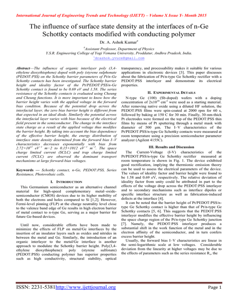
International Journal of Engineering Trends and Technology (IJETT) – Volume X Issue Y- Month 2015 The influence of surface state density at the interfaces of n-Ge Schottky contacts modified with conducting polymer Dr. A. Ashok Kumar# # Assistant Professor, Department of Physics Y.S.R. Engineering College of Yogi Vemana University, Proddatur, Andhra Pradesh, India. 1 drashok.yvuce@gmail.com Abstract—The influence of organic interlayer poly (3,4ethylene dioxythiophene) doped with poly (styrene sulphonate (PEDOT:PSS) on the Schottky barrier parameters of Pt/n-Ge Schottky contacts has been investigated. The Schottky barrier height and ideality factor of the Pt/PEDOT:PSS/n-Ge Schottky contact is found to be 0.69 eV and 1.58. The series resistance of the Schottky contacts is evaluated using Cheung and Cheung functions. It is more important to know how the barrier height varies with the applied voltage in the forward bias condition. Because of the potential drop across the interfacial layer, the zero bias barrier height is different from that expected in an ideal diode. Similarly the potential across the interfacial layer varies with bias because of the electrical field present in the semiconductor. The change in the interface state charge as a result of the applied voltage thus modifies the barrier height. By taking into account the bias dependence of the effective barrier height, the energy distribution of interface state density determined from the forward bias I–V characteristics decreases exponentially with bias from 2.72×10¹² eV−1 m−2 to 0.15×10¹² eV−1 m−2. The space charge limited current (SCLC) and trap charge limited current (TCLC) are observed the dominant transport mechanisms at large forward-bias voltages. Keywords — Schottky contact, n-Ge, PEDOT:PSS, Series Resistance, Photovoltaic cells. I. INTRODUCTION This Germanium semiconductor as an alternative channel material for high-speed complementary metal–oxidesemiconductor (CMOS) devices due to its higher mobility of both the electrons and holes compared to Si [1,2]. However, Fermi-level pinning (FLP) at the charge neutrality level close to the valence band edge of Ge results in high electron barrier of metal contact to n-type Ge, serving as a major barrier for future Ge-based devices. Until now, considerable efforts have been made to minimize the effects of FLP on metal/Ge interfaces by the insertion of an insulator layers such as oxides and nitrides in between the metal and Ge. Similarly, the introduction of an organic interlayer to the metal/Ge interface is another approach to modulate the Schottky barrier height. Poly(3,4ethylene dioxythiophene): poly (styrene sulfonate) (PEDOT:PSS) conducting polymer has superior properties such as high conductivity, structural stability, optical ISSN: 2231-5381http://www.ijettjournal.org transparency, and processability makes it suitable for various applications in electronic devices [3]. This paper discusses about the fabrication of Pt/n-type Ge Schottky rectifier with a PEDOT:PSS interlayer and demonstrate its electrical properties. II. EXPERIMENTAL DETAILS N-type Ge (100) (Sb-doped) wafers with a doping concentration of 2x1018 cm-3 were used as a starting material. After removing native oxide using a diluted HF solution, the PEDOT:PSS films were spin-coated at 2000 rpm for 60 s, followed by baking at 150 C for 30 min. Finally, 30-nm-thick Pt electrodes were formed on the top of the PEDOT:PSS thin films by means of Pt sputtering through a metal mask with diameter of 500 μm. The I–V characteristics of the Pt/PEDOT:PSS/n-type Ge Schottky contacts were measured at room temperature using a precision semiconductor parameter analyzer (Agilent 4155C). III. Results and Discussion The Current-Voltage (I-V) characteristics of the Pt/PEDOT:PSS/n-type Ge Schottky rectifier measured at room temperature is shown in Fig. 1. The device exhibited good rectification, implying the thermionic emission theory can be used to assess the electrical parameters of the device. The values of ideality factor and barrier height were found to be 1.58 and 0.69 eV, respectively. The relative deviation of ideality factor from unity could be attributed in part to the effects of the voltage drop across the PEDOT:PSS interlayer and to secondary mechanisms such as interface dipoles or specific interface structure as well as fabrication-induced defects at the interface [4]. It can be noted that the barrier height of Pt/PEDOT:PSS/ntype Ge Schottky contact is higher than that of Pt/n-type Ge Schottky contacts [5, 6]. This suggests that the PEDOT:PSS interlayer modifies the effective barrier height by influencing the space charge region of the Pt/n-type Ge Schottky junction [7]. Namely, the PEDOT:PSS interlayer produces a substantial shift in the work function of the metal and in the electron affinity of the semiconductor, and in turn confers excess barrier height. Usually, the forward bias I–V characteristics are linear in the semi-logarithmic scale at low voltages. Considerable deviation from the linearity at higher voltages may be due to the effects of parameters such as the series resistance R s, the Page 1 International Journal of Engineering Trends and Technology (IJETT) – Volume X Issue Y- Month 2015 interlayer is likely to retain forward current conduction in Pt/PEDOT:PSS/n-type Ge Schottky contact At high forward bias voltages, the trapped carriers provide reliable information about the conduction paths and the density of states which can be evaluated from the log-log scales of I-V characteristics. The forward-bias log(I) versus log(V) plot of the PEDOT:PSS/n-Ge Schottky contact is Fig 1. Forward and reverse bias current-voltage characteristics of Pt/PEDOT:PSS/n-type Ge Schottky contacts measured at room temperature. interfacial layer and interface states [8]. The parameter Rs is only effective in the downward-curvature region (non-linear region) of the forward I–V characteristics at sufficiently high applied voltage. At high currents, there is always a deviation of the ideality that has been clearly shown to depend on the interface state density and bulk series resistance, as one would expect. The lower the interface state density and the series resistance, the greater is the range over which ln I(V) does in fact yield a straight line. Furthermore, ideality factor (n) and the series resistance (Rs) were evaluated using a method developed by Cheung and Cheung. The series resistances extracted from the plot of dV/d(lnI) vs. I were almost identical to those from the plot of H(I) vs. I (shown in Fig.2), implying their consistency and validity. It should be noted that the series resistance of Pt/PEDOT:PSS/ntype Ge Schottky contact is much higher than that of Pt/n-type Ge Schottky contact [5]. This implies that the series resistance is a current-limiting factor for Pt/PEDOT:PSS/n-type Ge Schottky contact. In other words, the voltage drop across series resistance caused by the presence of an organic Fig 2. dV/d(lnI) vs. I and H(I) vs. I plots obtained from the forward I–V characteristics of the Pt/PEDOT:PSS/n-type Ge Schottky contacts. ISSN: 2231-5381http://www.ijettjournal.org Fig 3. Forward bias log (I) versus log(V) characteristics of Pt/PEDOT:PSS/n-Ge contacts shown in Figure 3. Figure shows the three distint regions in the forward-bias current-voltage characteristics. It is observed an ohmic region at low voltages up to a transition voltage of about 0.2V with a slope of about 1.28. At increased voltages current also increases which satisfies the relation IαVm where m varies with the injection level and trap charges distribution. The least square fit of region II shows a slope of about 5.61 which represents an exponential distribution of traps in the band gap of the organic material and the current conduction is purely due to Space charge limited current. The slope in the region III is found to be 3.35. The current conduction in region III could be associated with trap-filled limit. At higher voltages, the decreased slope is in region III than compared to region II may be due to the high injection level whose dependence is the same as in the trap charge limited current [9]. In n-type semiconductors, the energy of the interface states ESS with respect to the bottom of the conduction band at the surface of the semiconductor (EC-ESS) is plotted against the interface state density (NSS) in fig. 4. As seen from figure, it is observed that the exponential growth of the interface state density from midgap towards to the bottom of the conduction band in the range from (EC-0.352) to (EC-0.677) eV. The density distribution of the interface states of the Pt/PEDOT:PSS/n-Ge Schottky diode changes from 2.72×10¹² eV−1 m−2 to 0.15×10¹² eV−1 m−2. The interface layer, interface states and fixed charges between the polymeric organic compound/ Page 2 International Journal of Engineering Trends and Technology (IJETT) – Volume X Issue Y- Month 2015 semiconductor structures play an important role in the determination of the characteristic parameters of the devices which generally deviates the forward and reverse bias characteristics of the Pt/PEDOT:PSS/n-Ge from its ideal characteristics. 3.0 [3] [4] [5] Pt/PEDOT/n-Ge -2 NSS ( 10 eV m ) 2.5 [6] 12 -1 2.0 1.5 [7] 1.0 Y. Chen, K.S. Kang, K.J. Han, K.H. Yoo, J. Kim, ―Enhanced optical and electrical properties of PEDOT: PSS films by the addition of MWCNT-sorbitol‖ Synth. Met. Vol. 159, pp. 1701–1704, sept.2009. W. Monch, ―Barrier heights of real Schottky contacts explained by metal-induced gap states and lateral inhomogeneities‖ J. Vac. Sci. Technol. B, Vol. 17, pp.1867-1876, May 1999. A. Ashok Kumar, V. Rajagopal Reddy, V. Janardhanam, Min-Woo Seo, Hyobong Hong, Kyu-Sang Shin, Chel-Jong Choi, ―Electrical Properties of Pt/n-Ge Schottky Contact Modified using Copper Phthalocyanine (CuPc) Interlayer‖ J. Electrochem. Soc. Vol. 159, pp. H33–H37, 2012. A. Ashok Kumar, V. Rajagopal Reddy, V. Janardhanam, Hyun-Deok Yang, Hyung-Joong Yun, Chel-Jong Choi, ―Electrical properties of Pt/n-type Ge Schottky contact with PEDOT:PSS interlayer‖, J. Alloys Comp. Vol. 549, pp. 18-21, 2013. M. Cakar, N. Yildirim, S. Karatas, C. Temirci, A. Turut, “Currentvoltage and capacitance-voltage characteristics of Sn/rhodamine-101∕n- 0.5 0.0 0.35 0.40 0.45 0.50 0.55 0.60 0.65 0.70 0.75 Ec-ESS (eV) Fig 4. Energy distribution of the interface state density of Pt/PEDOT:PSS/n-Ge Schottky contacts. Briefly, polymeric organic/inorganic semiconductor diodes may be useful to increase the quality of devices fabricated by using the semiconductor in establishing processes for minimizing surface states, surface damage and contamination and actively tunable barrier heights. [8] [9] Si and Sn/rhodamine-101∕p-Si Schottky barrier diodes” J. Appl. Phys. Vol. 100, pp. 074505-74510, Oct. 2006. A.R.V. Roberts, D.A. Evans, ―Modification of GaAs Schottky diodes by thin organic interlayers’ Appl. Phys. Lett. Vol. 86, pp. 072105072107, Feb. 2005. T. Kılıcoglu, M.E. Aydın, G. Topal, M.A. Ebeoglu, H. Saygılı, ―The effect of a novel organic compound chiral macrocyclic tetraamide-I interfacial layer on the calculation of electrical characteristics of an Al/tetraamide-I/p-Si contact‖, Synthetic Metals vol. 157, pp. 540–545, July 2007. III. CONCLUSIONS The fabrication and analysis of distribution of surface states of Pt/PEDOT:PSS/n-Ge Schottky contacts has been investigated. The Schottky barrier height and ideality factor of the Pt/PEDOT:PSS/n-Ge Schottky contact is found to be 0.69 eV and 1.58. It is observed that the potential across the interfacial layer varies with bias because of the electrical field present in the semiconductor. The change in the interface state charge as a result of the applied voltage thus modifies the barrier height. The energy distribution of interface state density determined from the forward bias I–V characteristics decreases exponentially with bias from 2.72×10¹² eV −1 m−2 to 0.15×10¹² eV−1 m−2. The dominant transport mechanisms at large forward-bias voltages may be attributed to space charge limited current (SCLC) and trap charge limited current (TCLC) mechanisms. REFERENCES [1] [2] J. Oh, P. Majhi, H. Lee, O. Yoo, S. Banerjee, C.Y. Kang, J. Yang, R. Harris, H. Tseng, R. Jammy, ―Improved Electrical Characteristics of Ge-on-Si Field-Effect Transistors With Controlled Ge Epitaxial Layer Thickness on Si Substrates‖ IEEE Electron Device Lett. Vol. 28, pp. 1044–1046, Nov. 2007. T. Maeda, K. Ikeda, S. Nakaharai, T. Tezuka, N. Sugiyama, Y. Moriyama, S. Takagi, ―High mobility Ge-on-insulator p-channel MOSFETs using Pt germanide Schottky source/drain‖ IEEE Electron Device Lett. Vol. 26, pp. 102–104, Feb. 2005. ISSN: 2231-5381http://www.ijettjournal.org Page 3
