AD5547-EP Dual-Current Output, Parallel Input, 16-Bit Multiplying DAC with 4-Quadrant Resistors Data Sheet
advertisement
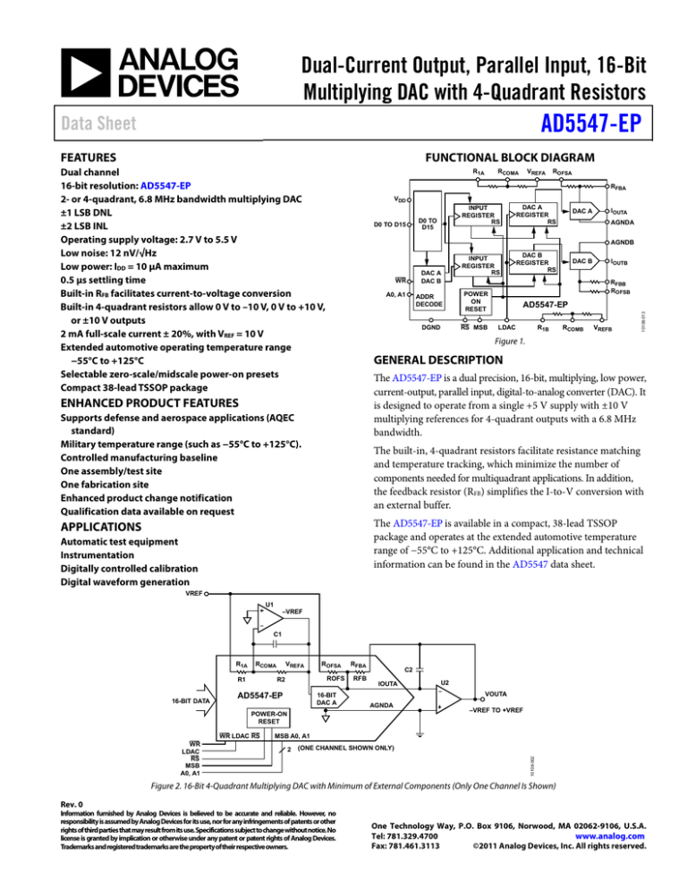
Dual-Current Output, Parallel Input, 16-Bit Multiplying DAC with 4-Quadrant Resistors AD5547-EP Data Sheet FEATURES FUNCTIONAL BLOCK DIAGRAM Dual channel 16-bit resolution: AD5547-EP 2- or 4-quadrant, 6.8 MHz bandwidth multiplying DAC ±1 LSB DNL ±2 LSB INL Operating supply voltage: 2.7 V to 5.5 V Low noise: 12 nV/√Hz Low power: IDD = 10 μA maximum 0.5 μs settling time Built-in RFB facilitates current-to-voltage conversion Built-in 4-quadrant resistors allow 0 V to –10 V, 0 V to +10 V, or ±10 V outputs 2 mA full-scale current ± 20%, with VREF = 10 V Extended automotive operating temperature range −55°C to +125°C Selectable zero-scale/midscale power-on presets Compact 38-lead TSSOP package R1A RCOMA VREFA ROFSA RFBA VDD D0 TO D15 D0 TO D15 INPUT REGISTER RS DAC A REGISTER RS INPUT REGISTER RS DAC B REGISTER RS DAC A IOUTA AGNDA AGNDB ADDR DECODE POWER ON RESET DGND RS MSB DAC B IOUTB RFBB ROFSB AD5547-EP LDAC R1B RCOMB VREFB 10108-013 WR A0, A1 DAC A DAC B Figure 1. GENERAL DESCRIPTION The AD5547-EP is a dual precision, 16-bit, multiplying, low power, current-output, parallel input, digital-to-analog converter (DAC). It is designed to operate from a single +5 V supply with ±10 V multiplying references for 4-quadrant outputs with a 6.8 MHz bandwidth. ENHANCED PRODUCT FEATURES Supports defense and aerospace applications (AQEC standard) Military temperature range (such as −55°C to +125°C). Controlled manufacturing baseline One assembly/test site One fabrication site Enhanced product change notification Qualification data available on request The built-in, 4-quadrant resistors facilitate resistance matching and temperature tracking, which minimize the number of components needed for multiquadrant applications. In addition, the feedback resistor (RFB) simplifies the I-to-V conversion with an external buffer. The AD5547-EP is available in a compact, 38-lead TSSOP package and operates at the extended automotive temperature range of −55°C to +125°C. Additional application and technical information can be found in the AD5547 data sheet. APPLICATIONS Automatic test equipment Instrumentation Digitally controlled calibration Digital waveform generation VREF U1 –VREF C1 R1A RCOMA R1 16-BIT DATA VREFA ROFSA ROFS R2 AD5547-EP 16-BIT DAC A RFBA RFB C2 IOUTA VOUTA AGNDA POWER-ON RESET –VREF TO +VREF MSB A0, A1 2 (ONE CHANNEL SHOWN ONLY) 10108-002 WR LDAC RS WR LDAC RS MSB A0, A1 U2 Figure 2. 16-Bit 4-Quadrant Multiplying DAC with Minimum of External Components (Only One Channel Is Shown) Rev. 0 Information furnished by Analog Devices is believed to be accurate and reliable. However, no responsibility is assumed by Analog Devices for its use, nor for any infringements of patents or other rights of third parties that may result from its use. Specifications subject to change without notice. No license is granted by implication or otherwise under any patent or patent rights of Analog Devices. Trademarks and registered trademarks are the property of their respective owners. One Technology Way, P.O. Box 9106, Norwood, MA 02062-9106, U.S.A. Tel: 781.329.4700 www.analog.com Fax: 781.461.3113 ©2011 Analog Devices, Inc. All rights reserved. AD5547-EP Data Sheet TABLE OF CONTENTS Features .............................................................................................. 1 Electrical Characteristics..............................................................3 Enhanced Product Features ............................................................ 1 Absolute Maximum Ratings ............................................................5 Applications....................................................................................... 1 ESD Caution...................................................................................5 Functional Block Diagram .............................................................. 1 Pin Configuration and Function Descriptions..............................6 General Description ......................................................................... 1 Typical Performance Characteristics ..............................................8 Revision History ............................................................................... 2 Outline Dimensions ....................................................................... 10 Specifications..................................................................................... 3 Ordering Guide .......................................................................... 10 REVISION HISTORY 9/11—Revision 0: Initial Version Rev. 0 | Page 2 of 12 Data Sheet AD5547-EP SPECIFICATIONS ELECTRICAL CHARACTERISTICS VDD = 2.7 V to 5.5 V, IOUT = virtual GND, GND = 0 V, VREF = −10 V to +10 V, TA = −55°C to +125°C, unless otherwise noted. Table 1. Parameter STATIC PERFORMANCE 1 Resolution Relative Accuracy Differential Nonlinearity Output Leakage Current Full-Scale Gain Error Bipolar Mode Gain Error Bipolar Mode Zero-Scale Error Full-Scale Temperature Coefficient 2 REFERENCE INPUT VREF Range REF Input Resistance R1 and R2 Resistance R1-to-R2 Mismatch Feedback and Offset Resistance Input Capacitance2 ANALOG OUTPUT Output Current Output Capacitance2 LOGIC INPUT AND OUTPUT Logic Input Low Voltage Logic Input High Voltage Symbol Test Conditions/Comments N INL DNL IOUT 1 LSB = VREF/216 = 153 μV at VREF = 10 V GFSE GE GZSE TCVFS VIL VDD = 5 V VDD = 3 V VDD = 5 V VDD = 3 V tDS Data to WR Hold Time tDH WR Pulse Width tWR LDAC Pulse Width tLDAC RS Pulse Width tRS WR to LDAC Delay Time tLWD SUPPLY CHARACTERISTICS Power Supply Range Positive Supply Current Power Dissipation Power Supply Sensitivity 8 Data = full scale Code dependent Input Leakage Current Input Capacitance2 INTERFACE TIMING2, 3 Data to WR Setup Time ±1 ±1 ±1 1 −18 4 4 IOUT COUT Max Unit ±2 ±1 10 20 ±5 ±5 ±4 Bits LSB LSB nA nA mV mV mV ppm/°C 5 5 ±0.5 10 5 +18 6 6 ±1.5 12 2 200 V kΩ kΩ Ω kΩ pF mA pF 0.8 0.4 2.4 2.1 IIL CIL VDD RANGE IDD PDISS PSS Typ 16 Monotonic Data = zero scale, TA = 25°C Data = zero scale, TA = TA maximum Data = full scale Data = full scale Data = full scale VREF REF R1 and R2 Δ(R1 to R2) RFB, ROFS CREF VIH Min 10 10 V V V V μA pF See Figure 3 VDD = 5 V VDD = 3 V VDD = 5 V VDD = 3 V VDD = 5 V 20 35 0 0 20 ns ns ns ns ns VDD = 3 V VDD = 5 V VDD = 3 V VDD = 5 V VDD = 3 V VDD = 5 V VDD = 3 V 35 20 35 20 35 0 0 ns ns ns ns ns ns ns 2.7 Logic inputs = 0 V Logic inputs = 0 V ∆VDD = ±5% Rev. 0 | Page 3 of 12 5.5 10 0.055 0.003 V μA mW %/% AD5547-EP Data Sheet Parameter AC CHARACTERISTICS 4 Output Voltage Settling Time Reference Multiplying Bandwidth DAC Glitch Impulse Multiplying Feedthrough Error Digital Feedthrough Total Harmonic Distortion Output Noise Density Analog Crosstalk Symbol Test Conditions/Comments tS To ±0.1% of full scale, data cycles from zero scale to full scale to zero scale VREF = 100 mV rms, data = full scale VREF = 0 V, midscale – 1 to midscale VREF = 100 mV rms, f = 10 kHz WR = 1, LDAC toggles at 1 MHz VREF = 5 V p-p, data = full scale, f = 1 kHz f = 1 kHz, BW = 1 Hz Signal input at Channel A and measures the output at Channel B, f = 1 kHz BW Q VOUT/VREF QD THD eN CAT Min 1 Typ Max Unit 0.5 μs 6.8 −3.5 −78 7 −104 12 −95 MHz nV-s dB nV-s dB nV/√Hz dB All static performance tests (except IOUT) are performed in a closed-loop system using an external precision OP97 I-to-V converter amplifier. The device RFB terminal is tied to the amplifier output. The +IN pin of the OP97 is grounded, and the IOUT of the DAC is tied to the OP97’s −IN pin. Typical values represent average readings measured at 25°C. 2 Guaranteed by design; not subject to production testing. 3 All input control signals are specified with tR = tF = 2.5 ns (10% to 90% of 3 V) and are timed from a voltage level of 1.5 V. 4 All ac characteristic tests are performed in a closed-loop system using an AD8038 I-to-V converter amplifier except for THD where the AD8065 was used. Timing Diagram tWR WR DATA tDS tDH tLWD LDAC tLDAC 10108-018 tRS RS Figure 3. AD5547-EP Timing Diagram Rev. 0 | Page 4 of 12 Data Sheet AD5547-EP ABSOLUTE MAXIMUM RATINGS Table 2. Parameter VDD to GND RFB, ROFS, R1, RCOM, and VREF to GND Logic Inputs to GND V(IOUT) to GND Input Current to Any Pin except Supplies Thermal Resistance (θJA)1 Maximum Junction Temperature (TJ MAX) Operating Temperature Range Storage Temperature Range Lead Temperature Vapor Phase, 60 sec Infrared, 15 sec 1 Rating –0.3 V to +8 V –18 V to +18 V –0.3 V to +8 V –0.3 V to VDD + 0.3 V ±50 mA 150°C −55°C to +125°C −65°C to +150°C Stresses above those listed under Absolute Maximum Ratings may cause permanent damage to the device. This is a stress rating only; functional operation of the device at these or any other conditions above those indicated in the operational section of this specification is not implied. Exposure to absolute maximum rating conditions for extended periods may affect device reliability. ESD CAUTION 215°C 220°C Package power dissipation = (TJ MAX − TA)/θJA. Rev. 0 | Page 5 of 12 AD5547-EP Data Sheet D1 1 38 D2 D0 2 37 D3 ROFSA 3 36 D4 RFBA 4 35 D5 R1A 5 34 D6 RCOMA 6 33 D7 VREFA 7 32 D8 31 D9 30 D10 29 VDD 28 D11 IOUTB 12 27 D12 VREFB 13 26 D13 RCOMB 14 25 D14 R1B 15 24 D15 RFBB 16 23 RS ROFSB 17 22 MSB WR 18 21 LDAC A0 19 20 A1 IOUTA 8 AGNDA 9 DGND 10 AGNDA 11 AD5547-EP TOP VIEW (Not to Scale) 10108-003 PIN CONFIGURATION AND FUNCTION DESCRIPTIONS Figure 4. Pin Configuration Table 3. Pin Function Descriptions Pin No. 1, 2, 24 to 28, 30 to 38 3 Mnemonic D0 to D15 Description Digital Input Data Bits D0 to D15. Signal level must be ≤ VDD + 0.3 V. ROFSA 4 5 RFBA R1A 6 RCOMA 7 VREFA 8 9 10 11 12 13 IOUTA AGNDA DGND AGNDB IOUTB VREFB 14 RCOMB 15 R1B 16 17 RFBB ROFSB 18 WR Bipolar Offset Resistor A. Accepts up to ±18 V. In 2-quadrant mode, ROFSA ties to RFBA. In 4-quadrant mode, ROFSA ties to R1A and the external reference. Internal Matching Feedback Resistor A. Connects to the external op amp for I-to-V conversion. 4-Quandrant Resistor. In 2-quadrant mode, R1A shorts to the VREFA pin. In 4-quadrant mode, R1A ties to ROFSA. Do not connect when operating in unipolar mode. Center Tap Point of the Two 4-Quadrant Resistors, R1A and R2A. In 4-quadrant mode, RCOMA ties to the inverting node of the reference amplifier. In 2-quadrant mode, RCOMA shorts to the associated VREFA pin. Do not connect if operating in unipolar mode. DAC A Reference Input in 2-Quadrant Mode, R2 Terminal in 4-Quadrant Mode. In 2-quadrant mode, VREFA is the reference input with constant input resistance vs. code. In 4-quadrant mode, VREFA is driven by the external reference amplifier. DAC A Current Output. Connects to the inverting terminal of external precision I-to-V op amp for voltage output. DAC A Analog Ground. Digital Ground. DAC B Analog Ground. DAC B Current Output. Connects to inverting terminal of external precision I-to-V op amp for voltage output. DAC B Reference Input Pin. Establishes DAC full-scale voltage. Constant input resistance vs. code. If configured with an external op amp for 4-quadrant multiplying, VREFB becomes –VREF. Center Tap Point of the Two 4-Quadrant Resistors, R1B and R2B. In 4-quadrant mode, RCOMB ties to the inverting node of the reference amplifier. In 2-quadrant mode, RCOMB shorts to the VREFB pin. Do not connect if operating in unipolar mode. 4-Quandrant Resistor. In 2-quadrant mode, R1B shorts to the VREFB pin. In 4-quadrant mode, R1B ties to ROFSB. Do not connect if operating in unipolar mode. Internal Matching Feedback Resistor B. Connects to external op amp for I-to-V conversion. Bipolar Offset Resistor B. Accepts up to ±18 V. In 2-quadrant mode, ROFSB ties to RFBB. In 4-quadrant mode, ROFSB ties to R1B and an external reference. Write Control Digital Input In, Active Low. WR transfers shift register data to the DAC register on the rising edge. Signal level must be ≤VDD + 0.3 V. Rev. 0 | Page 6 of 12 Data Sheet AD5547-EP Pin No. 19 20 21 22 Mnemonic A0 A1 LDAC MSB 23 RS 29 VDD Description Address Pin 0. Signal level must be ≤VDD + 0.3 V. Address Pin 1. Signal level must be ≤VDD + 0.3 V. Digital Input Load DAC Control. Signal level must be ≤VDD + 0.3 V. Power-On Reset State. MSB = 0 corresponds to zero-scale reset; MSB = 1 corresponds to midscale reset. The signal level must be ≤VDD + 0.3 V. Active low resets both input and DAC registers. Resets to zero-scale if MSB = 0 and resets to midscale if MSB = 1. Signal level must be ≤VDD + 0.3 V. Positive Power Supply Input. The specified range of operation is 2.7 V to 5.5 V. Table 4. Address Decoder Pins A1 0 0 1 1 A0 0 1 0 1 Output Update DAC A None DAC A and DAC B DAC B Table 5. Control Inputs RS WR LDAC Register Operation 0 1 1 1 1 X 0 1 0 X 0 1 1 1 1 0 Reset the output to 0 with MSB = 0; reset the output to midscale with MSB = 1. Load the input register with data bits. Load the DAC register with the contents of the input register. The input and DAC registers are transparent. When LDAC and WR are tied together and programmed as a pulse, the data bits are loaded into the input register on the falling edge of the pulse and are then loaded into the DAC register on the rising edge of the pulse. No register operation. Rev. 0 | Page 7 of 12 AD5547-EP Data Sheet TYPICAL PERFORMANCE CHARACTERISTICS 5 1.0 VDD = 5 V TA = 25° C 0.8 SUPPLY CURRENT I DD (LSB) 0.6 INL (LSB) 0.4 0.2 0 –0.2 –0.4 –0.6 4 3 2 1 0 8192 16,384 24,576 32,768 40,960 49,152 57,344 65,536 CODE (Decimal) 0 10108-019 –1.0 0 0.5 1.0 1.5 2.0 2.5 3.0 3.5 4.0 4.5 5.0 LOGIC INPUT VOLTAGE V IH (V) Figure 5. AD5547-EP Integral Nonlinearity Error 10108-023 –0.8 Figure 8. Supply Current vs. Logic Input Voltage 1.0 3.0 0.8 2.5 SUPPLY CURRENT (mA) 0.6 DNL (LSB) 0.4 0.2 0 –0.2 –0.4 –0.6 2.0 0x5555 1.5 0x8000 1.0 0xFFFF 0x0000 0.5 0 8192 16,384 24,576 32,768 40,960 49,152 57,344 65,536 CODE (Decimal) 0 10k 10108-020 –1.0 100k 1M 10M 100M CLOCK FREQUENCY (Hz) Figure 6. AD5547-EP Differential Nonlinearity Error 10108-024 –0.8 Figure 9. AD5547-EP Supply Current vs. Clock Frequency 1.5 90 VREF = 2.5 V TA = 25° C VDD = 5 V ± 10% VREF = 10V 80 1.0 0.5 PSRR (–dB) 60 INL 0 DNL –0.5 50 40 30 20 –1.0 GE 2 4 6 8 SUPPLY VOLTAGE V DD (V) 10 0 10 100 1k 10k FREQUENCY (Hz) 100k 1M Figure 10. Power Supply Rejection Ratio (PSRR) vs. Frequency Figure 7. Linearity Error vs. Supply Voltage, VDD Rev. 0 | Page 8 of 12 10108-014 –1.5 10 10108-022 LINEARITY ERROR (LSB) 70 Data Sheet AD5547-EP 2 0 LDAC 1 –2 GAIN (dB) –4 2 –6 –8 –10 –12 VOUT A CH1 2.70V B CH1 –6.20V 400.00ns –14 –16 –18 10k 100k 1M 10M 100M FREQUENCY (Hz) Figure 13. AD5547-EP Unipolar Reference Multiplying Bandwidth Figure 11. Settling Time from Full Scale to Zero Scale –3.85 –3.90 VOUT (V) –3.95 –4.00 –4.05 –4.10 –4.20 –20 –10 0 10 20 30 40 TIME (ns) 10108-016 –4.15 Figure 12. AD5547-EP Midscale Transition and Digital Feedthrough Rev. 0 | Page 9 of 12 10108-017 M 200ns 10108-025 CH1 5.00V CH2 2.00V AD5547-EP Data Sheet OUTLINE DIMENSIONS 9.80 9.70 9.60 20 38 4.50 4.40 4.30 6.40 BSC 1 19 PIN 1 1.20 MAX 0.15 0.05 COPLANARITY 0.10 0.50 BSC 0.27 0.17 SEATING PLANE 0.20 0.09 8° 0° 0.70 0.60 0.45 COMPLIANT TO JEDEC STANDARDS MO-153-BD-1 Figure 14. 38-Lead Thin Shrink Small Outline Package [TSSOP] (RU-38) Dimension s shown in millimeters ORDERING GUIDE Model 1 AD5547SRU-EP 1 Resolution (Bits) 16 DNL (LSB) ±1 INL (LSB) ±2 Temperature Range −55°C to +125°C Z = RoHS Compliant Part. Rev. 0 | Page 10 of 12 Package Description 38-Lead TSSOP Package Option RU-38 Data Sheet AD5547-EP NOTES Rev. 0 | Page 11 of 12 AD5547-EP Data Sheet NOTES ©2011 Analog Devices, Inc. All rights reserved. Trademarks and registered trademarks are the property of their respective owners. D10108-0-9/11(0) Rev. 0 | Page 12 of 12
