Current Output/Serial Input, 16-Bit DAC AD5543-EP Data Sheet
advertisement
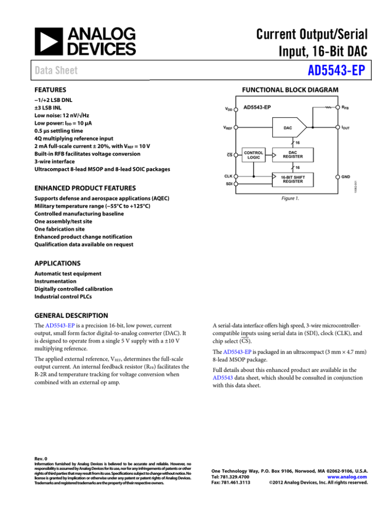
Current Output/Serial Input, 16-Bit DAC AD5543-EP Data Sheet FEATURES FUNCTIONAL BLOCK DIAGRAM VDD VREF Supports defense and aerospace applications (AQEC) Military temperature range (−55°C to +125°C) Controlled manufacturing baseline One assembly/test site One fabrication site Enhanced product change notification Qualification data available on request RFB IOUT DAC 16 CS CONTROL LOGIC DAC REGISTER 16 CLK ENHANCED PRODUCT FEATURES AD5543-EP SDI 16-BIT SHIFT REGISTER GND 10082-001 −1/+2 LSB DNL ±3 LSB INL Low noise: 12 nV/√Hz Low power: IDD = 10 μA 0.5 μs settling time 4Q multiplying reference input 2 mA full-scale current ± 20%, with VREF = 10 V Built-in RFB facilitates voltage conversion 3-wire interface Ultracompact 8-lead MSOP and 8-lead SOIC packages Figure 1. APPLICATIONS Automatic test equipment Instrumentation Digitally controlled calibration Industrial control PLCs GENERAL DESCRIPTION The AD5543-EP is a precision 16-bit, low power, current output, small form factor digital-to-analog converter (DAC). It is designed to operate from a single 5 V supply with a ±10 V multiplying reference. The applied external reference, VREF, determines the full-scale output current. An internal feedback resistor (RFB) facilitates the R-2R and temperature tracking for voltage conversion when combined with an external op amp. A serial-data interface offers high speed, 3-wire microcontrollercompatible inputs using serial data in (SDI), clock (CLK), and chip select (CS). The AD5543-EP is packaged in an ultracompact (3 mm × 4.7 mm) 8-lead MSOP package. Full details about this enhanced product are available in the AD5543 data sheet, which should be consulted in conjunction with this data sheet. Rev. 0 Information furnished by Analog Devices is believed to be accurate and reliable. However, no responsibility is assumed by Analog Devices for its use, nor for any infringements of patents or other rights of third parties that may result from its use. Specifications subject to change without notice. No license is granted by implication or otherwise under any patent or patent rights of Analog Devices. Trademarks and registered trademarks are the property of their respective owners. One Technology Way, P.O. Box 9106, Norwood, MA 02062-9106, U.S.A. Tel: 781.329.4700 www.analog.com Fax: 781.461.3113 ©2012 Analog Devices, Inc. All rights reserved. AD5543-EP Data Sheet TABLE OF CONTENTS Features .............................................................................................. 1 Timing Diagram ............................................................................4 Enhanced Product Features ............................................................ 1 Absolute Maximum Ratings ............................................................5 Applications....................................................................................... 1 ESD Caution...................................................................................5 Functional Block Diagram .............................................................. 1 Pin Configuration and Function Descriptions..............................6 General Description ......................................................................... 1 Typical Performance Characteristics ..............................................7 Revision History ............................................................................... 2 Outline Dimensions ..........................................................................9 Specifications..................................................................................... 3 Ordering Guide .............................................................................9 REVISION HISTORY 2/12—Revision 0: Initial Version Rev. 0 | Page 2 of 12 Data Sheet AD5543-EP SPECIFICATIONS VDD = 5 V ± 10%, VSS = 0 V, IOUT = virtual GND, GND = 0 V, VREF = 10 V, TA = full operating temperature range, unless otherwise noted. Table 1. Parameter STATIC PERFORMANCE 1 Resolution Relative Accuracy Differential Nonlinearity Output Leakage Current Full-Scale Gain Error Full-Scale Temperature Coefficient 2 REFERENCE INPUT VREF Range Input Resistance Input Capacitance2 ANALOG OUTPUT Output Current Output Capacitance2 LOGIC INPUTS AND OUTPUT Logic Input Low Voltage Logic Input High Voltage Input Leakage Current Input Capacitance2 INTERFACE TIMING2, 4 Clock Input Frequency Clock Width High Clock Width Low CS to Clock Setup Clock to CS Hold Data Setup Data Hold SUPPLY CHARACTERISTICS Power Supply Range Positive Supply Current Power Dissipation Power Supply Sensitivity AC CHARACTERISTICS4 Output Voltage Settling Time Reference Multiplying Bandwidth DAC Glitch Impulse Feedthrough Error Digital Feedthrough Total Harmonic Distortion Output Spot Noise Voltage Symbol Condition 5 V ± 10% Unit N INL DNL IOUT 1 LSB = VREF/216 = 153 μV when VREF = 10 V 16 ±3 −1/+2 10 20 ±1/±4 1 Bits LSB max LSB max nA max nA max mV typ/max ppm/°C typ −15/+15 5 5 V min/max kΩ typ 3 pF typ 2 200 mA typ pF typ VIL VIH IIL CIL 0.8 2.4 10 10 V max V min μA max pF max fCLK tCH tCL tCSS tCSH tDS tDH 50 10 10 0 10 5 10 MHz ns min ns min ns min ns min ns min ns min 4.5/5.5 10 0.055 0.006 V min/max μA max mW max %/% max 0.5 μs typ 6.6 7 −83 7 −103 12 MHz typ nV-sec dB nV-sec dB typ nV/√Hz GFSE TCVFS Monotonic Data = 0x0000, TA = 25°C Data = 0x0000, TA = TA maximum Data = 0xFFFF VREF RREF CREF IOUT COUT VDD RANGE IDD PDISS PSS tS BW Q VOUT/VREF Q THD eN Data = 0xFFFF Code dependent Logic inputs = 0 V Logic inputs = 0 V ΔVDD = ±5% To ±0.1% of full scale, Data = 0x0000 to 0xFFFF to 0x0000 VREF = 100 mV rms, data = 0xFFFF VREF = 0 V, data = 0x7FFF to 0x8000 Data = 0x0000, VREF = 100 mV rms, same channel CS = 1 and fCLK = 1 MHz VREF = 5 V p-p, data = 0xFFFF, f = 1 kHz f = 1 kHz, BW = 1 Hz 1 All static performance tests (except IOUT) are performed in a closed-loop system using an external precision OP177 I-to-V converter amplifier. The RFB terminal is tied to the amplifier output. The +IN op amp is grounded, and the DAC IOUT is tied to the −IN op amp. Typical values represent average readings measured at 25°C. These parameters are guaranteed by design and are not subject to production testing. 3 All ac characteristic tests are performed in a closed-loop system using an AD8038 I-to-V converter amplifier except for THD where an AD8065 was used. 4 All input control signals are specified with tR = tF = 2.5 ns (10% to 90% of 3 V) and timed from a voltage level of 1.5 V. 2 Rev. 0 | Page 3 of 12 AD5543-EP Data Sheet TIMING DIAGRAM SDI D15 D14 D13 D12 D11 D10 D9 D8 D1 D0 CLK tDS tDH tCH tCSS tCL tCSH 10082-016 CS Figure 2. Timing Diagram Rev. 0 | Page 4 of 12 Data Sheet AD5543-EP ABSOLUTE MAXIMUM RATINGS Table 2. Parameter VDD to GND VREF to GND Logic Inputs to GND V(IOUT) to GND Input Current to Any Pin Except Supplies Package Power Dissipation Thermal Resistance, θJA 8-Lead Surface Mount (MSOP) Maximum Junction Temperature (TJ Max) Operating Temperature Range Enhanced Plastic (EP Version) Storage Temperature Range Lead Temperature RM-8 (Vapor Phase, 60 sec) RM-8 (Infrared, 15 sec) Rating −0.3 V to +8 V −18 V to +18 V −0.3 V to +8 V −0.3 V to VDD + 0.3 V ±50 mA (TJ Max − TA)/θJA Stresses above those listed under Absolute Maximum Ratings may cause permanent damage to the device. This is a stress rating only; functional operation of the device at these or any other conditions above those indicated in the operational section of this specification is not implied. Exposure to absolute maximum rating conditions for extended periods may affect device reliability. ESD CAUTION 150°C/W 150°C −55°C to +125°C −65°C to +150°C 215°C 220°C Rev. 0 | Page 5 of 12 AD5543-EP Data Sheet CLK 1 8 CS SDI 2 AD5543-EP 7 VDD RFB 3 TOP VIEW (Not to Scale) 6 GND 5 IOUT VREF 4 10082-004 PIN CONFIGURATION AND FUNCTION DESCRIPTIONS Figure 3. Pin Configuration Table 3. Pin Function Descriptions Pin No. 1 2 3 4 5 Mnemonic CLK SDI RFB VREF IOUT 6 7 8 GND VDD CS Description Clock Input. Positive-edge triggered, clocks data into shift register. Serial Register Input. Data loads directly into the shift register MSB first. Extra leading bits are ignored. Internal Matching Feedback Resistor. This pin connects to an external op amp for voltage output. DAC Reference Input Pin. Establishes DAC full-scale voltage. Constant input resistance vs. code. DAC Current Output. This pin connects to the inverting terminal of the external precision I-to-V op amp for voltage output. Analog and Digital Ground. Positive Power Supply Input. Specified range of operation at 5 V ± 10%. Chip Select. Active low digital input. Transfers shift-register data to DAC register on rising edge. Rev. 0 | Page 6 of 12 Data Sheet AD5543-EP TYPICAL PERFORMANCE CHARACTERISTICS 5 1.0 VDD = 5V TA = 25°C 0.8 4 SUPPLY CURRENT I DD (mA) 0.6 INL (LSB) 0.4 0.2 0 –0.2 –0.4 3 2 1 –0.6 0 8192 16,384 24,576 32,768 40,960 49,152 57,344 65,536 CODE (Decimal) 0 10082-005 –1.0 0.5 0 1.0 1.5 2.0 2.5 3.0 3.5 4.0 5.0 4.5 LOGIC INPUT VOLTAGE VIH (V) Figure 4. Integral Nonlinearity Error 10082-010 –0.8 Figure 7. Supply Current, IDD vs. Logic Input Voltage, VIH 1.0 3.0 0.8 2.5 SUPPLY CURRENT (mA) 0.6 DNL (LSB) 0.4 0.2 0 –0.2 –0.4 2.0 0x5555 1.5 0x8000 1.0 0xFFFF 0x0000 –0.6 0.5 0 8192 16,384 24,576 32,768 40,960 49,152 57,344 65,536 CODE (Decimal) 0 10k Figure 5. Differential Nonlinearity Error 100k 1M 10M CLOCK FREQUENCY (Hz) 100M 10082-011 –1.0 10082-006 –0.8 Figure 8. Supply Current vs. Clock Frequency 90 1.5 VREF = 2.5V TA = 25°C VDD = 5V ± 10% VREF = 10V 80 1.0 60 PSRR (dB) 0.5 INL 0 DNL 50 40 30 –0.5 20 –1.5 GE 2 4 6 8 SUPPLY VOLTAGE V DD (V) 10 10 0 10 100 1k 10k FREQUENCY (Hz) 100k 1M Figure 9. Power Supply Rejection Ratio (PSRR) vs. Frequency Figure 6. Linearity Error vs. Supply Voltage, VDD Rev. 0 | Page 7 of 12 10082-012 –1.0 10082-009 LINEARITY ERROR (LSB) 70 AD5543-EP Data Sheet 20 –3.65 0 –3.70 –3.75 –40 VOUT (V) –3.80 –60 –80 –3.85 –3.90 –100 –3.95 –120 0 5 10 15 20 25 FREQUENCY (kHz) 10082-200 –160 –5V 5V 2V DLY 67.72µs 136ns –10 0 10 20 30 TIME (ns) Figure 12. Midscale Transition and Digital Feedthrough Figure 10. Analog Total Harmonic Distortion A2 –4.05 –20 Figure 11. Settling Time Rev. 0 | Page 8 of 12 40 10082-026 –4.00 –140 10082-014 POWER SPECTRUM (dB) –20 Data Sheet AD5543-EP OUTLINE DIMENSIONS 3.20 3.00 2.80 8 3.20 3.00 2.80 1 5.15 4.90 4.65 5 4 PIN 1 IDENTIFIER 0.65 BSC 0.95 0.85 0.75 15° MAX 1.10 MAX 0.40 0.25 6° 0° 0.23 0.09 COMPLIANT TO JEDEC STANDARDS MO-187-AA 0.80 0.55 0.40 10-07-2009-B 0.15 0.05 COPLANARITY 0.10 Figure 13. 8-Lead Mini Small Outline Package [MSOP] (RM-8) Dimensions shown in millimeters ORDERING GUIDE Model 1 , 2 AD5543SRMZ-EP 1 2 INL (LSB) ±3 RES (LSB) 16 Temperature Range −55°C to +125°C Package Description 8-Lead Mini Small Outline Package [MSOP] The AD5543 contains 1040 transistors. The die size measures 55 mil × 73 mil or 4,015 sq. mil. Z = RoHS Compliant Part. Rev. 0 | Page 9 of 12 Package Option RM-8 Branding DHR AD5543-EP Data Sheet NOTES Rev. 0 | Page 10 of 12 Data Sheet AD5543-EP NOTES Rev. 0 | Page 11 of 12 AD5543-EP Data Sheet NOTES ©2012 Analog Devices, Inc. All rights reserved. Trademarks and registered trademarks are the property of their respective owners. D10082-0-2/12(0) Rev. 0 | Page 12 of 12
