High Modulation Bandwidth Implant- Confined Photonic Crystal Vertical-Cavity Surface-Emitting Lasers
advertisement
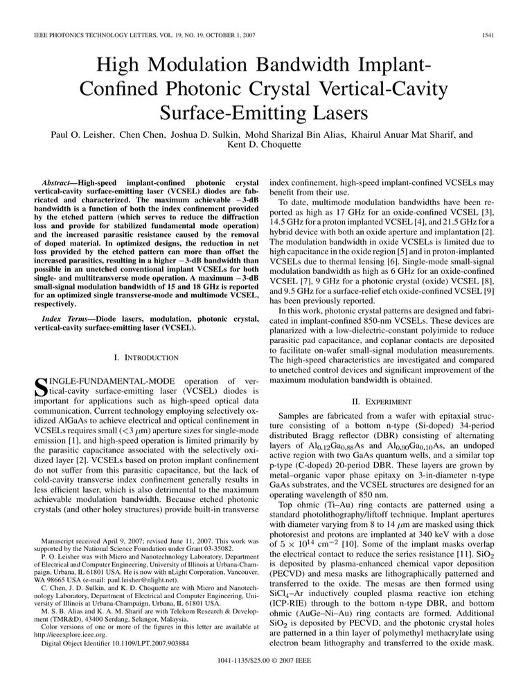
IEEE PHOTONICS TECHNOLOGY LETTERS, VOL. 19, NO. 19, OCTOBER 1, 2007 1541 High Modulation Bandwidth ImplantConfined Photonic Crystal Vertical-Cavity Surface-Emitting Lasers Paul O. Leisher, Chen Chen, Joshua D. Sulkin, Mohd Sharizal Bin Alias, Khairul Anuar Mat Sharif, and Kent D. Choquette Abstract—High-speed implant-confined photonic crystal vertical-cavity surface-emitting laser (VCSEL) diodes are fabricated and characterized. The maximum achievable 03-dB bandwidth is a function of both the index confinement provided by the etched pattern (which serves to reduce the diffraction loss and provide for stabilized fundamental mode operation) and the increased parasitic resistance caused by the removal of doped material. In optimized designs, the reduction in net loss provided by the etched pattern can more than offset the increased parasitics, resulting in a higher 03-dB bandwidth than possible in an unetched conventional implant VCSELs for both single- and multitransverse mode operation. A maximum 03-dB small-signal modulation bandwidth of 15 and 18 GHz is reported for an optimized single transverse-mode and multimode VCSEL, respectively. Index Terms—Diode lasers, modulation, photonic crystal, vertical-cavity surface-emitting laser (VCSEL). I. INTRODUCTION S INGLE-FUNDAMENTAL-MODE operation of vertical-cavity surface-emitting laser (VCSEL) diodes is important for applications such as high-speed optical data communication. Current technology employing selectively oxidized AlGaAs to achieve electrical and optical confinement in VCSELs requires small ( 3 m) aperture sizes for single-mode emission [1], and high-speed operation is limited primarily by the parasitic capacitance associated with the selectively oxidized layer [2]. VCSELs based on proton implant confinement do not suffer from this parasitic capacitance, but the lack of cold-cavity transverse index confinement generally results in less efficient laser, which is also detrimental to the maximum achievable modulation bandwidth. Because etched photonic crystals (and other holey structures) provide built-in transverse Manuscript received April 9, 2007; revised June 11, 2007. This work was supported by the National Science Foundation under Grant 03-35082. P. O. Leisher was with Micro and Nanotechnology Laboratory, Department of Electrical and Computer Engineering, University of Illinois at Urbana-Champaign, Urbana, IL 61801 USA. He is now with nLight Corporation, Vancouver, WA 98665 USA (e-mail: paul.leisher@nlight.net). C. Chen, J. D. Sulkin, and K. D. Choquette are with Micro and Nanotechnology Laboratory, Department of Electrical and Computer Engineering, University of Illinois at Urbana-Champaign, Urbana, IL 61801 USA. M. S. B. Alias and K. A. M. Sharif are with Telekom Research & Development (TMR&D), 43400 Serdang, Selangor, Malaysia. Color versions of one or more of the figures in this letter are available at http://ieeexplore.ieee.org. Digital Object Identifier 10.1109/LPT.2007.903884 index confinement, high-speed implant-confined VCSELs may benefit from their use. To date, multimode modulation bandwidths have been reported as high as 17 GHz for an oxide-confined VCSEL [3], 14.5 GHz for a proton implanted VCSEL [4], and 21.5 GHz for a hybrid device with both an oxide aperture and implantation [2]. The modulation bandwidth in oxide VCSELs is limited due to high capacitance in the oxide region [5] and in proton-implanted VCSELs due to thermal lensing [6]. Single-mode small-signal modulation bandwidth as high as 6 GHz for an oxide-confined VCSEL [7], 9 GHz for a photonic crystal (oxide) VCSEL [8], and 9.5 GHz for a surface-relief etch oxide-confined VCSEL [9] has been previously reported. In this work, photonic crystal patterns are designed and fabricated in implant-confined 850-nm VCSELs. These devices are planarized with a low-dielectric-constant polyimide to reduce parasitic pad capacitance, and coplanar contacts are deposited to facilitate on-wafer small-signal modulation measurements. The high-speed characteristics are investigated and compared to unetched control devices and significant improvement of the maximum modulation bandwidth is obtained. II. EXPERIMENT Samples are fabricated from a wafer with epitaxial structure consisting of a bottom n-type (Si-doped) 34-period distributed Bragg reflector (DBR) consisting of alternating layers of Al Ga As and Al Ga As, an undoped active region with two GaAs quantum wells, and a similar top p-type (C-doped) 20-period DBR. These layers are grown by metal–organic vapor phase epitaxy on 3-in-diameter n-type GaAs substrates, and the VCSEL structures are designed for an operating wavelength of 850 nm. Top ohmic (Ti–Au) ring contacts are patterned using a standard photolithography/liftoff technique. Implant apertures with diameter varying from 8 to 14 m are masked using thick photoresist and protons are implanted at 340 keV with a dose cm [10]. Some of the implant masks overlap of the electrical contact to reduce the series resistance [11]. SiO is deposited by plasma-enhanced chemical vapor deposition (PECVD) and mesa masks are lithographically patterned and transferred to the oxide. The mesas are then formed using SiCl –Ar inductively coupled plasma reactive ion etching (ICP-RIE) through to the bottom n-type DBR, and bottom ohmic (AuGe–Ni–Au) ring contacts are formed. Additional SiO is deposited by PECVD, and the photonic crystal holes are patterned in a thin layer of polymethyl methacrylate using electron beam lithography and transferred to the oxide mask. 1041-1135/$25.00 © 2007 IEEE 1542 IEEE PHOTONICS TECHNOLOGY LETTERS, VOL. 19, NO. 19, OCTOBER 1, 2007 Fig. 2. L–I –V characteristics of implant-confined photonic crystal VCSEL (Design B). The inset shows the single-mode lasing spectrum taken at maximum power. Fig. 1. Small-signal modulation response at several current injection levels for optimized implant-confined photonic crystal VCSELs. (a) Single-mode laser with a maximum 3-dB modulation bandwidth of 15 GHz; and (b) multimode laser with a maximum 3-dB bandwidth of 18 GHz. 0 0 For this parametric study on the high-speed modulation of our devices, we designed 20 different photonic crystal patterns, which in conjunction with different implant aperture sizes, produced more than 1000 unique device structures. The three particular photonic crystal patterns which showed the fastest modulation with period a and hole diameter are considered and m), Design B here: Design A ( and m), and Design C ( and ( m). The hole patterns are etched using SiCl –Ar ICP-RIE, and the remaining SiO is carefully removed. To reduce device parasitics and to facilitate on-wafer small-signal measurements, coplanar gold ground-signal-ground contacts are deposited on a 6- m-thick layer of photodefinable polyimide. The continuous-wave VCSEL light–current–voltage ( – – ) and spectral characteristics are measured using on-wafer probing at room temperature. At maximum power, each VCSEL is categorized as not lasing, multimode lasing, or single-mode lasing, where single-mode is defined as a single peak at the fundamental (lowest energy) wavelength and greater than 30-dB sidemode suppression ratio over the entire dynamic operating range of the VCSEL. The room-temperature small-signal modulation response was measured using a vector network analyzer. A cleaved fiber connected to a 25-GHz photodetector is positioned over the top of the VCSEL to collect light and carefully aligned to avoid feedback effects. The frequency where the modulation response decreases by 3 dB relative to its response at dc is measured for both single-mode and multimode VCSELs, which indicates the 3-dB modulation bandwidth or the optical bandwidth. III. RESULTS Fig. 1 shows the small-signal modulation response of a single-mode and multimode implant-confined photonic crystal VCSEL at a variety of injection levels. For the single-mode device, the maximum modulation bandwidth of 15 GHz is 0 Fig. 3. (a) Maximum 3-dB modulation bandwidth as a function of implant diameter for three single-mode photonic crystal designs (see text for details). The maximum bandwidth of unetched control devices is plotted for comparison, with the open circles/dashed lines corresponding to control devices which operate multimode. (b) Maximum 3-dB modulation bandwidth as function of implant diameter for VCSELs with overlapping contacts. All unetched control devices lased multimode. 0 achieved at 8 mA in Fig. 1(a), from photonic crystal Design B with an 11- m implant diameter. The maximum modulation bandwidth of a multimode implanted photonic crystal device is 18 GHz as shown in Fig. 1(b). This multimode photonic crystal VCSEL has an implant diameter of 12 m, and its photonic and m. The crystal design parameters are continuous-wave – – characteristics for the single-mode device that has achieved 15-GHz modulation bandwidth are shown in Fig. 2. This laser has a threshold current of 1.35 mA, a slope efficiency of 0.26 W/A, a series resistance of 137 , and maintains stable fundamental mode operation through rollover. The inset of Fig. 2 illustrates the optical spectrum of this optimized implant-confined photonic crystal VCSEL at maximum power. Fig. 3(a) illustrates the maximum 3-dB modulation bandwidth for the three different single-mode photonic crystal designs which are etched into VCSELs with varying implant diameter size. For all photonic crystal VCSELs, the defect diameter (defined by the holes) is smaller than the implant diameter. The LEISHER et al.: HIGH MODULATION BANDWIDTH IMPLANT-CONFINED PHOTONIC CRYSTAL VCSELs 0 Fig. 4. The 3-dB bandwidth versus the square root of the injection current minus the drive current for the optimized photonic crystal implant VCSEL and an unetched control implant VCSEL (open circles represent multimode lasing). maximum bandwidth for a series of unetched conventional implant VCSELs is also plotted in Fig. 3(a). VCSELs with implant diameters larger than 10- m lase multimode. The etching of the holes increases the series resistance of the VCSEL [12]. Hence, the difference in maximum modulation bandwidth for the three photonic crystal designs in Fig. 3(a) is due to the differences in both the differential series resistance and device efficiency caused by the etched holes. For example, the photonic crystal VCSEL with Design A has smaller hole diameter as compared to Designs B and C, and thus the resultant shallower etched holes and lower differential series resistance leads to higher modulation bandwidth in Fig. 3(a). The photonic crystal devices exhibit higher modulation bandwidths than the unetched control devices due to a reduction in diffraction loss which resulted in improved efficiency and decreased threshold [12]. To further reduce parasitic resistance and optimize high-speed performance, some devices are fabricated with the implant aperture overlapping the contact metal [11]. This overlap reduces the series resistance by increasing the conductive path through unimplanted (undamaged) semiconductor. The maximum 3-dB modulation bandwidth for these optimized devices is shown in Fig. 3(b). All unetched implant VCSELs with overlapping contacts lase multimode. Fig. 4 plots the 3-dB bandwidth versus the square root of the injection current above threshold for the optimized photonic crystal implant VCSEL and an unetched control implant VCSEL with the same size implant aperture diameter. The control implant VCSEL begins lasing multimode for mA . Neglecting the effects of parasitics, the relaxation oscillation frequency scales with the 3-dB frequency. Since the photon density is proportional to the output power (which is proportional to injection current above threshold), Fig. 4 is expected to exhibit linear behavior. The slope of the linear fit gives the modulation current efficiency factor (MCEF) [5]. The measured MCEF for the optimized implant-confined photonic crystal VCSEL is 6.4 GHz/mA , which is greater than what has been observed for an implant VCSEL. The improvement in MCEF for the etched photonic crystal implant VCSEL relative to the unetched implant VCSEL indicates that the reduction in loss due to the index confinement more than compensates for the increased parasitic series resistance. IV. CONCLUSION High-speed single-mode implant-confined photonic crystal VCSELs are fabricated and characterized. The maximum achievable 3-dB bandwidth is a function of both the index 1543 confinement provided by the etched pattern (which serves to reduce the diffraction loss) and the increased parasitic resistance caused by the removal of doped material. In optimized designs, the reduction in net loss provided by the etched pattern can more than offset the increased parasitics, resulting in a higher MCEF and 3-dB bandwidth than possible in an unetched conventional implant VCSEL. A maximum 15- and 18-GHz small-signal modulation bandwidth is reported for single-mode and multimode VCSELs, respectively. These results are achieved with an electrical aperture diameter of 11 and 12 m, respectively, which are larger than the oxide diameter generally reported for high-speed multimode oxide-confined VCSELs, and significantly larger than that required for single-mode operation in oxide-confined VCSELs. Because device reliability depends strongly on current density [13], it is expected that implant-confined photonic crystal VCSELs are potentially more reliable than single-mode VCSELs fabricated utilizing small oxide apertures. REFERENCES [1] C. Jung, R. Jäger, M. Grabherr, P. Schnitzer, R. Michalzik, B. Weigl, S. Muller, and K. J. Ebeling, “4.8 mW single-mode oxide confined top-surface emitting vertical-cavity laser diodes,” Electron. Lett., vol. 33, no. 21, pp. 1790–1791, 1997. [2] K. L. Lear, V. M. Hietala, H. Q. Hou, M. Ochiai, J. J. Banas, B. E. Hammons, J. C. Zolper, and S. P. Kilcoyne, “Small and large signal modulation of 850 nm oxide-confined vertical cavity surface emitting lasers,” in OSA Trends in Optics and Photonics, Advances in Vertical Cavity Surface Emitting Lasers, C. J. Chang-Hasnain, Ed. Washington, DC: Optical Society of America, 1997, vol. 15, pp. 69–74. [3] A. N. Al-Omari and K. L. Lear, “Polyimide-planarized vertical-cavity surface-emitting lasers with 17.0-GHz bandwidth,” IEEE Photon. Technol. Lett., vol. 16, no. 4, pp. 969–971, Apr. 2004. [4] Y. Satuby and M. Orenstin, “Limits of the modulation response of a single mode proton implanted VCSEL,” IEEE Photon. Technol. Lett., vol. 10, no. 6, pp. 760–762, Jun. 1998. [5] K. L. Lear, A. Mar, K. D. Choquette, S. P. Kilcoyne, R. P. Schneider, Jr., and K. M. Geib, “High-frequency modulation of oxide-confined vertical cavity surface emitting lasers,” Electron. Lett., vol. 32, pp. 457–458, 1996. [6] K. L. Lear, R. P. Schneider, Jr., K. D. Choquette, and S. P. Kilcoyne, “Index guiding dependent effects in implant and oxide confined vertical cavity surface emitting lasers,” IEEE Photon. Technol. Lett., vol. 8, no. 6, pp. 740–742, Jun. 1996. [7] C. Carlsson, H. Martinsson, R. Schatz, J. Halonen, and A. Larsson, “Analog modulation properties of oxide confined VCSELs at microwave frequencies,” J. Lightw. Technol., vol. 20, no. 9, pp. 1740–1749, Sep. 2002. [8] T. S. Kim, A. J. Danner, D. M. Grasso, E. W. Young, and K. D. Choquette, “Single fundamental mode photonic crystal vertical cavity surface emitting laser with 9 GHz bandwidth,” Electron. Lett., vol. 40, no. 21, pp. 1340–1342, 2004. [9] E. Soderberg, P. Modh, J. S. Gustavsson, A. Larsson, Z. Z. Zhang, J. Berggren, and M. Hammar, “Single mode 1.28 m InGaAs VCSELs using an inverted surface relief,” in Proc. 2006 IEEE Int. Semiconductor Laser Conf., 2006, Paper WC5. [10] K. D. Choquette and K. M. Geib, “Fabrication and performance of vertical-cavity surface-emitting lasers,” in Vertical-Cavity Surface-Emitting Lasers, Wilmsen, Temkin, and Coldren, Eds. New York: Cambridge, 1999, pp. 193–232. [11] G. Hasnain, K. Tai, L. Yang, Y. H. Wang, R. J. Fischer, J. D. Wynn, B. Weir, N. K. Dutta, and A. Y. Cho, “Performance of gain-guided surface emitting lasers with semiconductor distributed Bragg reflectors,” IEEE J. Quantum Electron., vol. 27, no. 6, pp. 1377–1385, Jun. 1991. [12] P. O. Leisher, A. J. Danner, J. J. Raftery, Jr., D. F. Siriani, and K. D. Choquette, “Loss and index guiding in single mode proton-implanted holey vertical-cavity surface-emitting lasers,” IEEE J. Quantum Electron., vol. 42, no. 10, pp. 1091–1096, Oct. 2006. [13] B. M. Hawkins, R. A. Hawthorne, III, J. K. Guenter, J. A. Tatum, and J. R. Biard, “Reliability of various size oxide aperture VCSELs,” in Proc. 52nd Electronic Components and Technology Conf., 2002, pp. 540–550.
