AN-610 Application Note

AN-610
Application Note
One Technology Way • P.O.
Box 9106 • Norwood, MA 02062-9106, U.S.A.
• Tel: 781.329.4700
• Fax: 781.461.3113
• www.analog.com
The PGA on Σ-Δ ADCs
by Adrian Sherry
INTRODUCTION
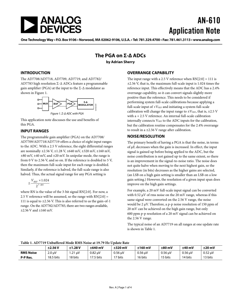
The AD7708/AD7718, AD7709, AD7719, and AD7782/
AD7783 high resolution Σ-Δ ADCs feature a programmable gain amplifier (PGA) at the input to the Σ-Δ modulator as
MUX BUF PGA
Σ ∆
MODULATOR
Figure 1. Σ-Δ ADC with PGA
This application note discusses the use and benefits of this PGA.
INPUT RANGES
The programmable gain amplifier (PGA) on the AD7708/
AD7709/AD7718/AD7719 offers a choice of eight input ranges to the ADC. With a 2.5 V reference, the eight differential ranges are nominally ±2.56 V, ±1.28 V, ±640 mV, ±320 mV, ±160 mV,
±80 mV, ±40 mV, and ±20 mV. In unipolar mode, the range is from 0 V to 2.56 V, and so on. If the reference is doubled to 5 V, then the maximum full-scale input for each range is doubled.
Similarly, if the reference is halved, the full-scale range is also halved. Thus, the actual signal range for any PGA setting is
±
V
REF
×
1
2 7
−
RN
.
024 where RN is the value of the 3-bit signal RN[2:0]. For now, a
2.5 V reference will be assumed, so the range with RN[2:0] =
111 is equal to ±2.56 V. This is also referred to as the gain-of-1 range. On the AD7782/AD7783, there are two ranges available,
±2.56 V and ±160 mV.
OVERRANGE CAPABILITY
The input range with a 2.5 V reference when RN[2:0] = 111 is
±2.56 V, that is, the maximum full-scale input is 1.024 times the reference input. This effectively means that the ADC has a 2.4% overrange capability, so it can convert signals slightly more positive than the reference. This needs to be considered if performing system full-scale calibrations because applying a full-scale input of +V
REF
and initiating a system full-scale calibration will change the input range to ±V
REF
, that is, ±2.5 V with a + 2.5 V reference. An internal full-scale calibration internally connects V
REF
to the ADC inputs for the calibration, but the calibration routine compensates for the 2.4% overrange to result in a ±2.56 V range after calibration.
NOISE/RESOLUTION
The primary benefit of having a PGA is that the noise, in terms of μF, decreases when the gain is increased. In effect, the input signal is gained up before being applied to the ADC, but the noise contribution is not gained up to the same extent, so there is an improvement in the signal-to-noise ratio. The noise does not quite halve when moving to the next highest gain, so the resolution (in bits) decreases as the higher gains are selected,
(an LSB on a high gain setting is smaller than an LSB on a low gain setting.) However, the resolution of a given input span does improve on the high gain settings.
For example, a 20 mV full-scale input signal can be converted with 0.52 μV of rms noise on the 20 mV range, whereas if this same signal were converted on the 2.56 V range, the noise would be 2 μV. Therefore, a p-p noise resolution of 150 ppm of
20 mV can be achieved on the high gain range, but only
600 ppm p-p resolution of a 20 mV signal can be achieved on the 2.56 V range.
The typical noise of an AD7719 on all ranges at one update rate
Table 1. AD7719 Unbuffered Mode RMS Noise at 19.79 Hz Update Rate
RMS Noise
P-P Res.
±2.56 V
2.0 μV
18.5 bits
±1.28 V
1.21 μV
18 bits
±640 mV
0.82 μV
17.5 bits
±320 mV
0.56 μV
17 bits
±160 mV
0.56 μV
16 bits
±80 mV
0.56 μV
15 bits
±40 mV
0.56 μV
14 bits
±20 mV
0.52 μV
13 bits
Rev. A | Page 1 of 4
AN-610
TABLE OF CONTENTS
Input Ranges...................................................................................... 1
Overrange Capability ....................................................................... 1
Noise/Resolution .............................................................................. 1
Revision History ............................................................................... 2
REVISION HISTORY
1/11—Rev. 0 to Rev. A
Updated Format..................................................................Universal
Changes to Input Currents Section ................................................ 4
2/03—Revision 0: Initial Version
Application Note
Range Matching.................................................................................3
Offset Register....................................................................................3
Input Currents ...................................................................................4
Rev. A | Page 2 of 4
Application Note
OFFSET ERRORS
A problem with changing ranges on many other ADCs with
PGAs is that the ADC offset may change with range, so offset calibrations are generally necessary after changing gain. However, with this family of chopped ADCs, the ADC offset error is insignificant, so there is no appreciable change in ADC offset when changing to another range. If the AD7708 or AD7718 is used with chopping disabled, offset calibrations should be performed when the range is changed.
RANGE MATCHING
Previous implementations of PGAs have partially relied on techniques such as binarily weighted circuit elements that are selectively switched in or out as the gain is changed. Because of manufacturing mismatches between these components, the gain does not exactly scale by two when the range is changed, meaning that an analog input will convert to different values depending on which gain is selected.
This family of ADCs from Analog Devices, Inc., uses a proprietary switching scheme to implement the PGA by using scaled sampling rates. This yields excellent matching between the different ranges, that is, a given analog input converts to a very similar value on different ranges. The specification on range matching is ±2 μV typical, which means there will typically be only a ±2 μV difference between conversion results of a fixed input on any of the eight ranges. (Note that this refers to the average dc result of a number on conversions rather than just a single reading, since the peak-to-peak noise on the 2.56 V range is greater than 2 μV.)
The combination of very small offset error and accurate gain matching greatly simplifies the process of auto ranging using the ADC. If the input signal is low level, it can be converted with maximum resolution on a high gain setting, but if the signal overranges the ADC, then the next lower gain setting can be selected and used immediately, without recalibrating the ADC.
Figure 2 illustrates a 19.92 mV signal being converted across all
eight ranges. No offset or gain calibrations are performed when the range changes. As can be seen, the mean code only varies by
2 μV to 3 μV across the eight ranges.
AN-610
19.928
19.926
19.924
19.922
19.920
19.918
0 1 2 3 4 5 6
RN
Figure 2. Range Matching Across All Ranges
7
CALIBRATIONS
A major advantage of accurate gain tracking is that an ADC calibration performed at one gain setting is also valid on the other gain settings. Previously, most ADCs with a PGA had to be recalibrated whenever the gain was changed, which reduced the ADC throughput; now a single ADC gain calibration is suffi cient. This allows the ADC to be calibrated in the factory on the
2.56 V range and used on any other range without recalibrating.
The AD7708/AD7718/AD7719 do have an internal ADC calibration mode available, but this should only be necessary if the ADC is operating at conditions significantly different from the factory calibration conditions given in the data sheet. The expected change in gain can be determined from the PSR and gain drift vs. temperature specifications in the data sheet. If the maximum expected change in gain is higher than the error budget for the application, then recalibration can be performed periodically.
OFFSET REGISTER
One situation on the AD7708/AD7718/AD7719 in which the
ADC can produce apparently different conversion results on different ranges is if the offset register contains a value other than the default 8000(00)H, as a result of a system offset calibration or by writing into the offset register. The weight of an offset register LSB depends on the selected range, so a value
8001(00)H removes twice as much offset on the 2.56 V range than on the 1.28 V range. If a system offset calibration were performed on one range with a nonzero analog input to the
ADC, there would be nonzero ADC results if the same input were to be converted on another range. Therefore, care must be taken when changing range if the offset register contains something other than the default 8000(00)H.
Rev. A | Page 3 of 4
AN-610
INPUT CURRENTS
The PGA varies the input and reference sampling rates in implementing the various gains, altering the dynamic load presented by the switched capacitor circuit. This could lead to gain and/or linearity errors due to external source impedances.
However, with a buffer present at the ADC input prior to the
PGA, minimal current is drawn by the analog inputs, and this current does not vary with input range. The AD7719 can operate with the buffer bypassed, so it is important to take care with external resistor and capacitor combinations in this case.
The reference sampling rate seen at the pin is fixed at 524 kHz for the 2.56 V to 320 mV ranges, and the reference sampling capacitor is also fixed, so there is no variation in reference current across these ranges. Therefore, any gain error due to resistance on the reference input remains fixed across these ranges.
If the reference current varied with range, any gain error caused by external resistance/capacitance on the reference would vary with range, so the benefit of having an ADC with excellent range matching could be lost. The reference current on these
Application Note
ADCs does vary at higher gain ranges, so care needs to be taken if the PGA gain is changed and there are external impedances on the reference input.
A
IN
(+)
A
IN
(–)
1nA MAX BUF
C
IN f
IN
= 64kHz – 524kHz
REF
IN
(+)
REF
IN
(–)
C
REF f
REF
= 524kHz
Figure 3. Input and Reference Model
SUMMARY
The PGA on this family of ADCs offers the benefit of higher resolution/lower noise at high gains, but without the disadvantage of requiring regular calibration every time the range is changed.
A buffered input and a new reference sampling scheme avoid many of the problems associated with previous multirange ADCs.
©2003–2011 Analog Devices, Inc. All rights reserved. Trademarks and
registered trademarks are the property of their respective owners.
AN03183-0-1/11(0)
Rev. A | Page 4 of 4


