Low‐Power High‐Speed Analog‐to‐Digital Converters with SES Calibration
advertisement
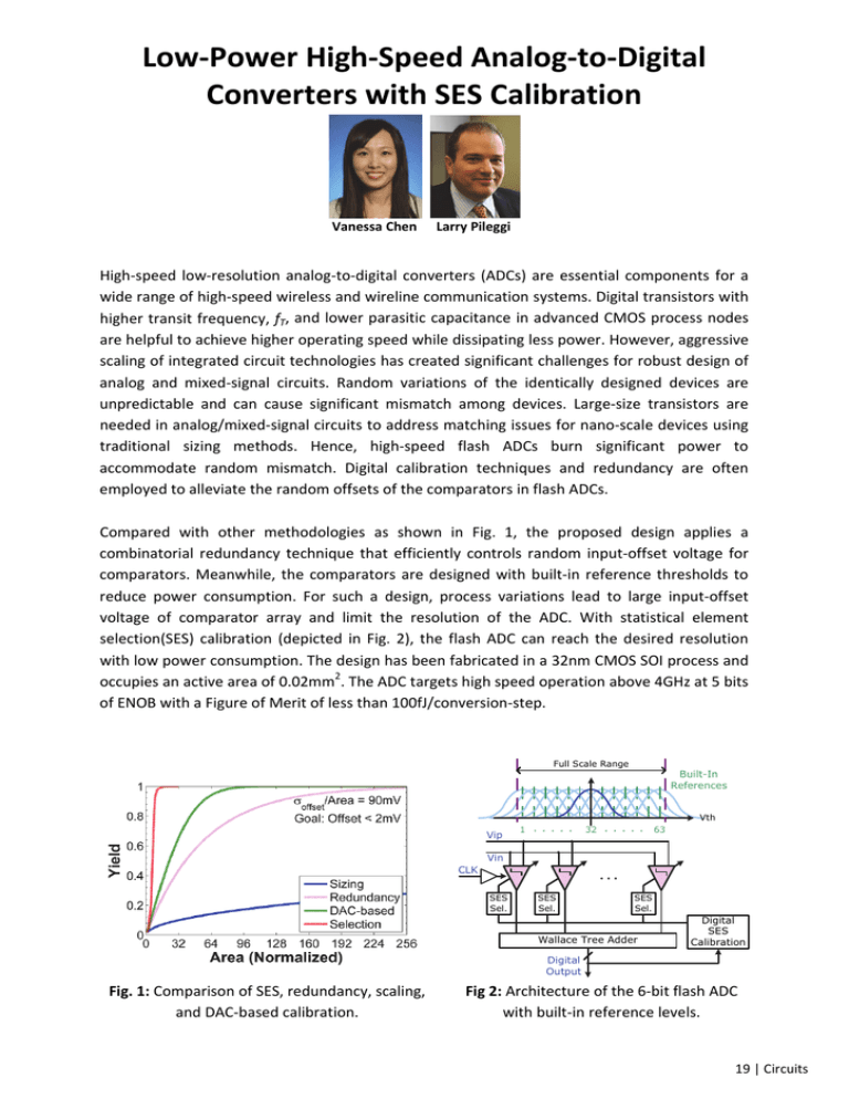
Low‐Power High‐Speed Analog‐to‐Digital Converters with SES Calibration Vanessa Chen Larry Pileggi High‐speed low‐resolution analog‐to‐digital converters (ADCs) are essential components for a wide range of high‐speed wireless and wireline communication systems. Digital transistors with higher transit frequency, fT, and lower parasitic capacitance in advanced CMOS process nodes are helpful to achieve higher operating speed while dissipating less power. However, aggressive scaling of integrated circuit technologies has created significant challenges for robust design of analog and mixed‐signal circuits. Random variations of the identically designed devices are unpredictable and can cause significant mismatch among devices. Large‐size transistors are needed in analog/mixed‐signal circuits to address matching issues for nano‐scale devices using traditional sizing methods. Hence, high‐speed flash ADCs burn significant power to accommodate random mismatch. Digital calibration techniques and redundancy are often employed to alleviate the random offsets of the comparators in flash ADCs. Compared with other methodologies as shown in Fig. 1, the proposed design applies a combinatorial redundancy technique that efficiently controls random input‐offset voltage for comparators. Meanwhile, the comparators are designed with built‐in reference thresholds to reduce power consumption. For such a design, process variations lead to large input‐offset voltage of comparator array and limit the resolution of the ADC. With statistical element selection(SES) calibration (depicted in Fig. 2), the flash ADC can reach the desired resolution with low power consumption. The design has been fabricated in a 32nm CMOS SOI process and 2 occupies an active area of 0.02mm . The ADC targets high speed operation above 4GHz at 5 bits of ENOB with a Figure of Merit of less than 100fJ/conversion‐step. Full Scale Range Built-In References Vth Vip 1 32 63 Vin CLK SES Sel. SES Sel. SES Sel. Wallace Tree Adder Digital SES Calibration Digital Output Fig. 1: Comparison of SES, redundancy, scaling, and DAC‐based calibration. Fig 2: Architecture of the 6‐bit flash ADC with built‐in reference levels. 19 | Circuits


