Harnessing plasmonics for solar cells commentary | focus
advertisement
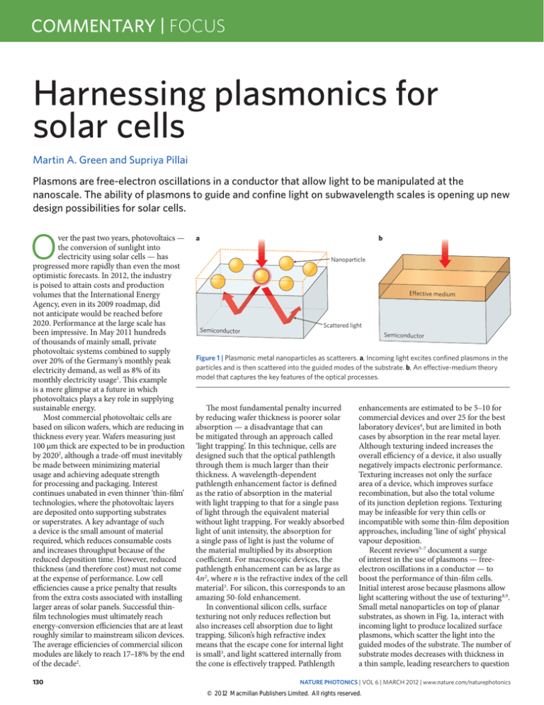
commentary | focus Harnessing plasmonics for solar cells Martin A. Green and Supriya Pillai Plasmons are free-electron oscillations in a conductor that allow light to be manipulated at the nanoscale. The ability of plasmons to guide and confine light on subwavelength scales is opening up new design possibilities for solar cells. O ver the past two years, photovoltaics — the conversion of sunlight into electricity using solar cells — has progressed more rapidly than even the most optimistic forecasts. In 2012, the industry is poised to attain costs and production volumes that the International Energy Agency, even in its 2009 roadmap, did not anticipate would be reached before 2020. Performance at the large scale has been impressive. In May 2011 hundreds of thousands of mainly small, private photovoltaic systems combined to supply over 20% of the Germany’s monthly peak electricity demand, as well as 8% of its monthly electricity usage1. This example is a mere glimpse at a future in which photovoltaics plays a key role in supplying sustainable energy. Most commercial photovoltaic cells are based on silicon wafers, which are reducing in thickness every year. Wafers measuring just 100 μm thick are expected to be in production by 20202, although a trade-off must inevitably be made between minimizing material usage and achieving adequate strength for processing and packaging. Interest continues unabated in even thinner ‘thin-film’ technologies, where the photovoltaic layers are deposited onto supporting substrates or superstrates. A key advantage of such a device is the small amount of material required, which reduces consumable costs and increases throughput because of the reduced deposition time. However, reduced thickness (and therefore cost) must not come at the expense of performance. Low cell efficiencies cause a price penalty that results from the extra costs associated with installing larger areas of solar panels. Successful thinfilm technologies must ultimately reach energy-conversion efficiencies that are at least roughly similar to mainstream silicon devices. The average efficiencies of commercial silicon modules are likely to reach 17–18% by the end of the decade2. 130 a b Nanoparticle Effective medium Semiconductor Scattered light Semiconductor Figure 1 | Plasmonic metal nanoparticles as scatterers. a, Incoming light excites confined plasmons in the particles and is then scattered into the guided modes of the substrate. b, An effective-medium theory model that captures the key features of the optical processes. The most fundamental penalty incurred by reducing wafer thickness is poorer solar absorption — a disadvantage that can be mitigated through an approach called ‘light trapping’. In this technique, cells are designed such that the optical pathlength through them is much larger than their thickness. A wavelength-dependent pathlength enhancement factor is defined as the ratio of absorption in the material with light trapping to that for a single pass of light through the equivalent material without light trapping. For weakly absorbed light of unit intensity, the absorption for a single pass of light is just the volume of the material multiplied by its absorption coefficient. For macroscopic devices, the pathlength enhancement can be as large as 4n2, where n is the refractive index of the cell material3. For silicon, this corresponds to an amazing 50-fold enhancement. In conventional silicon cells, surface texturing not only reduces reflection but also increases cell absorption due to light trapping. Silicon’s high refractive index means that the escape cone for internal light is small3, and light scattered internally from the cone is effectively trapped. Pathlength enhancements are estimated to be 5–10 for commercial devices and over 25 for the best laboratory devices4, but are limited in both cases by absorption in the rear metal layer. Although texturing indeed increases the overall efficiency of a device, it also usually negatively impacts electronic performance. Texturing increases not only the surface area of a device, which improves surface recombination, but also the total volume of its junction depletion regions. Texturing may be infeasible for very thin cells or incompatible with some thin-film deposition approaches, including ‘line of sight’ physical vapour deposition. Recent reviews5–7 document a surge of interest in the use of plasmons — freeelectron oscillations in a conductor — to boost the performance of thin-film cells. Initial interest arose because plasmons allow light scattering without the use of texturing 8,9. Small metal nanoparticles on top of planar substrates, as shown in Fig. 1a, interact with incoming light to produce localized surface plasmons, which scatter the light into the guided modes of the substrate. The number of substrate modes decreases with thickness in a thin sample, leading researchers to question nature photonics | VOL 6 | MARCH 2012 | www.nature.com/naturephotonics © 2012 Macmillan Publishers Limited. All rights reserved. Focus | commentary whether the same light-trapping limits would apply as to macroscopic specimens. Initial results were not encouraging: researchers predicted that reducing the substrate thickness would progressively lower the light trapping efficacy. Over the past five years, much has been learned about how to exploit these confined plasmons effectively. For example, researchers found that interference between scattered and incoming light reduces (perhaps counterintuitively) the overall reflection of a device. Effective-medium theories have proved their usefulness in the field of metamaterials and can be used to describe this interference at least qualitatively 10 (Fig. 1b), although a number of caveats still apply 11. Introducing reflective nanoparticles into a dielectric increases its effective refractive index. Recent work suggests that aluminium particles may be more effective than noble metals for reducing reflection12. This advantage is attributed to the higher resonant frequency of aluminium, as particles absorb light at wavelengths below their resonance frequency. This led to the suggestion that the rear side of the cell is the most effective location for plasmonic scatterers7. Recent work7,13,14 has clarified the effect of particle shape and spacer layers for both front and rear locations. Hemispheres and cylinders are superior to the spheres shown in Fig. 1a because they have a larger contact area with the silicon substrate. Surface plasmon polaritons (SPPs) have recently been shown to be active in this contact area13. SPPs are plasmon modes that propagate along metal–dielectric interfaces over distances determined by absorption in the metal. Using SPPs propagating along the rear surface of a cell to enhance cell absorption (Fig. 2a) is also under active investigation5. These SPPs can be excited at visible wavelengths, where the magnitude of the real (negative) component of the metal’s dielectric constant becomes larger than the corresponding (positive) value for the dielectric. In terms of refractive indices, this corresponds roughly to the imaginary part of the metal’s index km becoming larger in magnitude than the real part of the dielectric (or, in this case, semiconductor) index ns. Evanescent waves decay in both the metal and the dielectric, but extend further into the dielectric by the inverse ratio of respective dielectric constants, which is roughly (km/ns)2. At a wavelength of 800 nm, evanescent fields extend around 17 nm into silver and 38 nm into crystalline silicon, where a long decay length is desirable because it increases absorption there5. A common concern5,6 has been whether metal absorption might override the benefits of semiconductor absorption. a b Evanescent wave Substrate mode Textured surface High-index layers Low-index layer SPP Metal reflector Metal reflector Figure 2 | Trapping light using evanescent waves. a, Features on the rear layer of a solar cell can not only scatter light into substrate modes but also excite SPPs propagating along the rear surface reflector. b, Evanescent states at the interface of a low-index medium embedded in high-index material can significantly boost absorption in a thin low-index layer. This problem can be explored by examining the reduction of plasmon propagation distance caused by absorption in the semiconductor. The fractional semiconductor absorption found in this way is given by fs = kskm3/(ns3nm + kskm3), where ns (nm) and ks (km) are the real and imaginary parts of the semiconductor (metal) indices. Only when ks > ns3nm/km3 will half of the propagating energy be absorbed in the semiconductor. Metals with a small value of nm/km3 maximize desirable absorption in the semiconductor. The fraction of incident perpendicular light that is reflected from the surface of a metal in vacuum, R, is given approximately by 1 − (4nm/km2). R therefore provides a simple screening parameter because km is relatively independent of the metal at visible wavelengths. The optical constants of metal candidates are often obtained from data in Palik’s handbook15, or from earlier data derived by Johnson and Christy 16. For silver, however, there are large differences between these data. Nash and Sambles17 rejected both data sets because they were derived from silver samples exposed to air, and instead tabulated an alternative ‘best set of values’ in the range of 400–900 nm. These give a silver vacuum reflectivity of 98.9% at 800 nm, whereas values from Palik and Johnson and Christy give 98.0% and 99.5%, respectively. Although these values are all relatively similar, small differences magnify to give a large difference in the calculated SPP light-trapping effectiveness. Handbook R values for gold, copper, aluminium and molybdenum (used in chalcogenide cells) at 800 nm are 97.4%, 96.3%, 86.8% and 55.6%, respectively, thus clearly identifying silver as the material of choice. Nash and Sambles17 measured nm = 0.087 and km = 5.48 at 800 nm, which suggests that SPP light trapping is effective only for absorption coefficients of more than 4,000 cm–1 for inorganic semiconductors. Organic semiconductors have smaller values of ns, which makes organic cells more promising candidates than inorganic cells. As explained by Schiff 18, these SPP modes represent photon-accessible states that are in addition to those involving propagation across the substrate. Photon coupling between both sets of states would potentially allow macroscopic light-trapping limits to be exceeded. Schiff calculated that the limits, neglecting metal absorption, could be increased to 4n2 + nλ/W, where W is the device thickness and λ is the wavelength of light. Rear gratings or rear-surface features such as those shown in Fig. 2a not only scatter light into substrate propagation modes, but also provide the required coupling. As noted above, metal absorption largely negates these gains18, although there may be scope for more optimal trade-offs5. Another way of describing potential gains in this geometry is through the local density of optical states19 ρ(r, ω) as a function of position, r, and radial frequency, ω, which can be determined from the local density of electromagnetic energy U(r, ω) = ρ(r, ω)hω/(exp(hω/kT) − 1), where hω and kT are the photon energy and thermal energy, respectively. In a dielectric near a metal interface, the local density of optical states increases due to the presence of additional evanescent modes, with ρ(r, ω) peaking at the SPP resonant frequency 19. Light trapping can be significantly improved by employing the geometry shown in Fig. 2b20, as the evanescent states at the interface between dielectrics of different refractive indices can enhance the local density of optical states. Trapping in a thin low-index (nL) layer immersed in high-index (nH) material boosts the macroscopic limit of 4nL2 by a further factor of (2nH/nL + nH5/nL5)/3, which equals 12 for nH/nL = 2. Yu et al. nature photonics | VOL 6 | MARCH 2012 | www.nature.com/naturephotonics © 2012 Macmillan Publishers Limited. All rights reserved. 131 commentary | focus a b Nanoparticle ITO (55 nm) Ag (20 nm) a-Si (15 nm) Ag (50 nm) Semiconductor junction Figure 3 | Plasmonic solar cell approaches. a, Metal nanoparticles embedded in the absorber at a cell junction enhance the electric field — and therefore light absorption — around their periphery. b, Unit cell of a recently proposed metamaterial–plasmonic cell consisting of, from top to bottom, an indium tin oxide (ITO) antireflection coating (55 nm), a silver top contact (20 nm) in an ‘over-full’ conducting chequer-board pattern, a thin layer of amorphous silicon (15 nm) as the active cell material and a rear silver reflector (50 nm). subsequently more simply derived this formula as well as a similar expression for embedded nanospheres21, showing smaller boosts in this case. Conversely, light trapping is suppressed for high-index media immersed in low-index materials, which emphasizes the importance of local environments in determining optical performance for thin high-index layers. This effect is well-documented for photoluminescence22, which is closely related to absorption through fundamental reciprocity relationships23. Performance can also be enhanced by positioning the metal nanoparticles to maximize absorption in the most active cell regions6,24 (Fig. 3a). The downside of this technique is that metal–semiconductor interfaces are regions of detrimental electronic activity. The introduction of intervening thin insulator layers may overcome this effect 24, albeit at the expense of diluting the associated field strength. Embedded nanoparticles might also be beneficial for promoting processes such as upconversion, which rise nonlinearly with increasing field strength. Much progress has been made in understanding the photovoltaic potential of plasmonics, and further work may uncover even more substantial gains. Figure 3b shows the structure of a recently proposed metamaterial–plasmonic solar cell25 that is simulated to give good performance with an extremely thin 15 nm amorphous-silicon active layer. The design of this cell was based on effective-medium theory analysis and then confirmed by full solutions to Maxwell’s equations. The structure involves 132 a 20-nm-thick top silver metal contact in an ‘over-full’ chequer-board pattern of subwavelength dimensions, which obscures 54% of the cell. The underlying 15-nm-thick amorphous silicon layer has a 50-nm-thick silver rear reflector. The top surface is covered in a 55-nm-thick indium tin oxide antireflection coating, resulting in a total device thickness of only 140 nm. The possible plasmonic activity in this structure is complex. The structure relies on extraordinary optical transmission through the top metallization holes26. Periodicity in the top contact geometry provides phase matching that allows SPP excitation, which contributes to both light transmission and scattering. The top silver layer is partly transmissive, which enables SPP stimulation on both of its sides. Although SPP stimulation on both sides is generally detrimental to extraordinary optical transmission, researchers were nevertheless able to measure26 reasonable transmission through holes similar to the subwavelength hole arrays of ref. 25, albeit at lower levels than in simulations. The amorphous silicon layer is so thin that coupling also occurs between the front and rear silver layers, leading to SPP excitation in the rear silver layer. Simulations suggest that this structure would absorb sufficient photons from the standard solar spectrum to give a current output of 19.7 mA cm–2, compared with 16.8 mA cm–2 from today’s highest-efficiency amorphous-silicon cell27. However, this simulation used Johnson and Christy optical parameters, and therefore possibly underestimates silver’s absorption losses by up to a factor of four. Full solutions to Maxwell’s equations will be crucial in unravelling the performance of increasingly complex geometries such as the one described above, and effectivemedium theory approximations may have a role in identifying structures that warrant detailed assessment. Localized plasmons have already demonstrated their potential to boost the performance of solar cells for cases when traditional texturing may not be viable. For propagating plasmons, parasitic optical absorption in the metallic structure and strong optical absorption near high-recombination metal–semiconductor interfaces both remain significant challenges. Nonetheless, plasmonics is opening up a new optical world at the subwavelength scale that is largely unexplored. High-index, non-absorbing dielectrics and the emerging field of metamaterial plasmonics may both offer new photovoltaic possibilities. The low cell thickness that is possible with plasmonics may not only deliver anticipated material savings but also ultimately allow the successful implementation of advanced high-performance concepts, such as hotcarrier cells28. ❒ Martin A. Green and Supriya Pillai are at the ARC Photovoltaics Centre of Excellence, University of New South Wales, Sydney, New South Wales 2052, Australia. e-mail: m.green@unsw.edu.au References 1.www.transparency.eex.com/en/ 2.www.itrpv.net/doc/roadmap_itrpv_2011_brochure_web.pdf 3. Yablonovitch, E. J. Opt. Soc. Am. 72, 899–907 (1982). 4. Green, M. A. Prog. Photovoltaics 17, 183–189 (2009). 5. Atwater, H. & Polman, A. Nature Mater. 9, 205–213 (2010). 6. Mallick, S. B., Sergeant, N. P., Agrawal, M., Lee, J.‑Y. & Peumans, P. MRS Bull. 36, 453–460 (2011). 7. Catchpole, K. R. et al. MRS Bull. 36, 461–467 (2011). 8. Stuart, H. R. & Hall, D. G. Appl. Phys. Lett. 69, 2327–2329 (1996). 9. Pillai, S. et al. J. Appl. Phys. 101, 093105 (2007). 10.Akimov, Y. A., Ostrikov, K. & Li, E. P. Plasmonics 4, 107–113 (2009). 11.Simovski, C. R. J. Opt. 13, 013001 (2011). 12.Akimov, Y. A. & Koh, W. S. Nanotechnology 21, 235201 (2010). 13.Beck, F. J., Mokkapati, S. & Catchpole, K. R. Opt. Express 19, 25230–25241 (2011). 14.Pillai, S., Beck, F. J., Catchpole, K. R., Ouyang, Z. & Green, M. A. J. Appl. Phys. 109, 073105 (2011). 15.Palik, E. D. (ed.) Handbook of Optical Constants of Solids (Academic, 1985). 16.Johnson, P. B. & Christy, R. W. Phys. Rev. B 6, 4370–4379 (1972). 17.Nash, D. J. & Sambles, J. R. J. Mod. Opt. 43, 81–91 (1996). 18.Schiff, E. A. J. Appl. Phys. 110, 104501 (2011). 19.Joulain, K., Carminati, R., Mulet, J.‑P. & Greffet, J.‑J. Phys. Rev. B 68, 245405 (2003). 20.Green, M. A. Prog. Photovoltaics 19, 473–477 (2011). 21.Yu, Z., Raman, A. & Fan, S. Proc. Natl Acad. Sci. USA 107, 17491–17496 (2010). 22.Yablonovitch, E., Gmitter, T. J. & Bhat, R. Phys. Rev. Lett. 61, 2546–2549 (1988). 23.Rau, U. Phys. Rev. B 76, 085303 (2007). 24.Lee, J.‑Y. & Peumans, P. Opt. Express 18, 10078–10087 (2010). 25.Wang, Y. et al. Nano Lett. 12, 440–445 (2012). 26.Braun, J., Gompf, B., Weiss, T., Giessen, H. & Dressel, M. Phys. Rev. B 84, 155419 (2011). 27.Green, M. A., Emery, K., Hishikawa, Y., Warta, W. & Dunlop, E. D. Prog. Photovoltaics 20, 12–20 (2012). 28.Aliberti, P. et al. J. Appl. Phys. 108, 094507 (2010). nature photonics | VOL 6 | MARCH 2012 | www.nature.com/naturephotonics © 2012 Macmillan Publishers Limited. All rights reserved.
