Influence of photonic nanotexture on the light extraction efficiency of GaN
advertisement
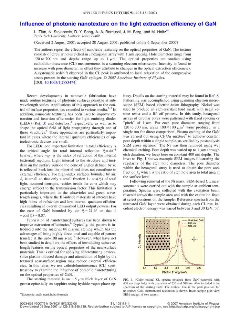
APPLIED PHYSICS LETTERS 91, 103115 共2007兲 Influence of photonic nanotexture on the light extraction efficiency of GaN L. Tian, N. Stojanovic, D. Y. Song, A. A. Bernussi, J. M. Berg, and M. Holtza兲 Texas Tech University, Lubbock, Texas 79409 共Received 2 August 2007; accepted 20 August 2007; published online 6 September 2007兲 The authors report the effects of nanoscale texturing on the optical properties of GaN. The texture consists of circular holes etched in a hexagonal array with 1 m spacing. Hole diameters range from 120 to 700 nm and depths range up to 1 m. The optical properties are studied using cathodoluminescence 共CL兲 measurements in a scanning electron microscope. Intensity is found to increase with pore diameter, an effect they attribute to changes in the optical extraction efficiencies. A systematic redshift observed in the CL peak is attributed to local relaxation of the compressive stress present in the starting GaN epilayer. © 2007 American Institute of Physics. 关DOI: 10.1063/1.2783474兴 Recent developments in nanoscale fabrication have made routine texturing of photonic surfaces possible at subwavelength scales. Applications of this approach to the control of surface properties has extended to various media.1–3 In addition, nanoscale texturing has been used to improve extraction and insertion efficiencies for light emitting diodes 共LEDs兲 共Ref. 3兲 and detectors,4 respectively, as well as to shape the optical field of light propagating through one of these structures.5 These approaches are particularly important in cases where the internal quantum efficiencies of optoelectronic devices are small. For LEDs, one important limitation in total efficiency is the critical angle for total internal reflection c = sin−1 共n2 / n1兲, where n1共2兲 is the index of refraction of the internal 共external兲 medium. Light internal to the structure and incident on the surface outside the cone of angles defined by c is reflected back into the material and does not contribute to external efficiency. For high-index surfaces bounded by air, c is small so that only a small fraction 1 − cos共c兲 of total light, assumed isotropic, resides inside the cone which may emerge subject to the transmission factor. This limitation is particularly important in the ultraviolet and green wavelength ranges, where the III-nitride materials of interest have high index of refraction and low internal quantum efficiencies resulting in overall diminished LED output powers. For the case of GaN bounded by air c ⬃ 21.6° so that 1 − cos共c兲 ⬃ 0.07. Fabrication of nanotextured surfaces has been shown to improve extraction efficiencies.6 Typically, the pattern is introduced into the material by plasma etching which has the advantages of being highly directional and capable of pattern transfer at the sub-100 nm scale.7 However, what have not been studied in detail are the effects of introducing subwavelength features on the optical properties of the near-surface materials. This is critical for applying nanotexturing devices, since plasma induced damage and attenuation of light by the textured near-surface region may reduce external efficiencies. In this letter, we use cathodoluminescence 共CL兲 spectroscopy to examine the influence of photonic nanotexturing on the optical properties of GaN. The starting material is an ⬃5 m thick layer of GaN grown epitaxially on sapphire using hydride vapor-phase epa兲 Electronic mail: mark.holtz@ttu.edu itaxy. Details on the starting material may be found in Ref. 8. Patterning was accomplished using scanning electron microscope 共SEM兲 based electron-beam lithography. Nickel was used to produce an etch-resistant hard mask with negativetone resist and a lift-off process. In this study, hexagonal arrays of circular pores were patterned with fixed spacing or “pitch” of 1 m. For each pore diameter, ranging from 120 to 700 nm, areas 100⫻ 100 m2 were produced in a single run for direct comparison. Plasma etching of the GaN was carried out using Cl2 / Ar mixture9 to achieve constant pore depth within a single sample, as verified by postanalysis SEM cross sections.7 The Ni was then removed using wet chemical etching. Pore depth was varied up to 1 m through etch duration; we focus here on constant 400 nm depths. The inset to Fig. 1 shows example SEM images illustrating the regularity of the etch hole diameters. The pore diameter within the hexagonal array is used to obtain the pore area fraction f A which is the ratio of etch hole area to total area at the surface level. Following removal of the Ni mask, SEM-based CL measurements were carried out with the sample at ambient temperature. Spectra were collected with the excitation beam rastered across the sample area and with the excitation fixed at select positions on the sample. Reference spectra from the untreated GaN layer were obtained during each CL run. Incident electron energy was varied between 3 and 30 keV, but FIG. 1. 共Color online兲 CL spectra obtained from GaN patterned with 400 nm deep holes with diameters of 250 and 500 nm. Also included is the spectrum of the starting GaN. The vertical line is the peak position for unstrained GaN. Instrumental resolution is shown. Inset: sample plan-view SEM images of two arrays. 0003-6951/2007/91共10兲/103115/3/$23.00 91, 103115-1 © 2007 American Institute of Physics Downloaded 06 Sep 2007 to 129.118.248.139. Redistribution subject to AIP license or copyright, see http://apl.aip.org/apl/copyright.jsp 103115-2 Tian et al. Appl. Phys. Lett. 91, 103115 共2007兲 FIG. 3. 共Color online兲 CL peak position vs area fraction for 400 nm deep hole arrays. The inset shows an example FEA simulation of stress at the surface. The curve shows the simulated weighted-average stress. FIG. 2. Normalized CL intensity with etched area fraction for 400 nm deep hole arrays with 1 m pitch. Dash-dot and dash curves show calculated intensity, each normalized to unetched GaN, originating from regions 1 and 2 in the inset, respectively. The combined factors are shown as the solid curve. we restrict our attention to 7 keV measurements since they address the optical properties of the near-surface 共⬃100 nm兲 GaN. Lateral spatial resolution at this energy is estimated to be 艋100 nm. Representative spectra are shown in Fig. 1 following the formation of 250 and 500 nm holes. Also included is the CL spectrum of the starting GaN material. For comparing intensities, specific areas with a given pore diameter region were imaged and CL data were taken before moving to the next area of the sample. The spectra in Fig. 1 show the main CL band, corresponding to the free exciton emission,10 which serves as a good measure of the energy gap. The CL peak of the starting material is blueshifted from that of a relaxed GaN reference sample by ⬃9.2 meV. Based on published dependences of the GaN energy gap,11 this shift corresponds to ⬃380 MPa of biaxial compressive stress. This value is consistent with 350± 40 MPa biaxial compressive stress determined from our Raman measurements and is attributed to combined residual and thermal expansion mismatch with the sapphire substrate.12 Also observed in Fig. 1 is an increase in emission intensity following the formation of pores. Figure 2 shows the dependence of CL intensity on pore diameter with pitch and depth fixed at 1 m and 400 nm, respectively, each normalized to the intensity of the starting material. Intensity enhancement is observed with a greater area fraction. This enhancement is attributed to changes in extraction efficiencies,13 and has been utilized for improving emission efficiencies in LEDs.14 In our experiments, the CL is generated in the near-surface volume of GaN excited by the electron beam. As depicted in the inset of Fig. 2, the volume which contributes to the CL emission is considered to consist of two regions, corresponding to the top surface 共1兲 and the pore bottoms 共2兲. In region 1 the light extraction depends on f A through two factors. The first factor is the effective medium which decreases the index of refraction for the porous layer, thereby producing a larger extraction cone through 1 − cos共c兲 described above, and increases the transmission factor of the pore layer/air interface. We apply here the Maxwell-Garnett effective medium approximation, which has been found to describe accurately the optical properties of media with nanopores.6 The second factor is 共1 − f A兲, which quantifies the remaining unetched region 1 material. Region 2 will also contribute to the measured emission intensity. Light emitted in region 2 and emanating toward the surface will be affected by transmission factors at the GaN/nanoporous layer and nanoporous layer/air interfaces. Transmission factors are calculated using the Fresnel relations. Based on these considerations, the net intensity may be expressed as I = I1 + I2 ⬀ 关共1 − f A兲1CL⌽e兴 + 关f A2CL⌽e兴, 共1兲 where 1共2兲 is the optical extraction efficiency for light originating in region 1共2兲, CL represents the intrinsic efficiency of the CL process in GaN, and ⌽e is the incident SEM electron flux. For a uniform GaN layer, this reduces to GaNCL⌽e, where GaN takes into account the light extraction cone and the internal optical transmission factor for GaN. Normalizing the right-hand side of Eq. 共1兲 to this factor, we calculate the emission ratio for each term shown as the curves labeled 1 and 2 in Fig. 2. As expected, the first term in Eq. 共1兲 is dominant. The combined effect in Fig. 2 is seen to agree well with the observed trend illustrating that the light extraction properties are described based on the effective medium and these straightforward considerations. We also observe shifts in the CL emission energy following the production of nanopores. In Fig. 3, we summarize the shift for the same series of nanopores discussed in Fig. 2. The CL peak of a relaxed GaN reference sample has an energy of 3.148 eV. The CL peak redshifts with increasing pore diameter 共f A兲, an effect we attribute to the local relaxation of the compressive stress in the nanopore region of the GaN. To check this interpretation, we carried out threedimensional simulations of the stress profile using finite element analysis 共FEA兲.15 The simulation includes the substrate, unetched epitaxial GaN, and the etch holes. Elastic constants for GaN are taken from Ref. 16 and the stress in the simulated layer matches the measured material. In the inset of Fig. 3, we show a sample plan-view FEA stress profile. The Downloaded 06 Sep 2007 to 129.118.248.139. Redistribution subject to AIP license or copyright, see http://apl.aip.org/apl/copyright.jsp 103115-3 Appl. Phys. Lett. 91, 103115 共2007兲 Tian et al. compressive stress is seen to relax in the pore regions, particularly near the hole edges. As expected, the relaxation becomes more pronounced with increasing f A. The CL emission preferentially arises from the recombination of electrons in the lowest available conduction state with holes in the highest lying valence state. For our case, the starting material is under compressive biaxial stress which widens the energy gap. Based on this, we expect CL to favor the GaN which is relaxed by the etching. In addition, the measurement will emphasize the near-surface region corresponding to the combined attenuation of electrons and emitted photons. However, this does not mean that only the fully relaxed GaN at the hole corners will participate, since the exciton diffusion lengths are also ⬍100 nm 共Ref. 17兲 and the distance from excitation to hole edge varies throughout the measurement. In Fig. 3, we compare average in-plane compressive stress in the near-surface 100 nm with the CL data. The stress average is calculated using an exponential weighting factor and published optical attenuation factors.18,19 Agreement with the observed trend in Fig. 3 is good, suggesting that stress relaxation is the primary reason for the observed shift in the GaN CL peak. We note that deeper 共1 m兲 holes result in faster observed and simulated relaxation with f A, as expected from the greater removal of the neighboring support of the unetched material. The deeper etching process also results in a slight broadening of the CL bands particularly near the hole edges, an effect we attribute to etch-induced damage.20 Focusing the SEM excitation at the bottom of the 400 nm etch holes results in a CL spectrum which is not affected by the process, suggesting that the damage has no cumulative effect on the optical properties of the GaN. In summary, we have studied the effects of nanoscale pore arrays on the optical properties of GaN. The introduction of these pores results in the enhancement of the emission intensity seen in CL measurements. The enhancement is described based on the effects of the nanopore array on emission primarily from the unetched component of the GaN along with a smaller contribution from the pore bottoms. Shifts observed in the CL emission are attributed to relaxation of the compressive stress present in the epilayer. FE simulations show that stress relaxation increases with etch hole diameter. Since the original stress is compressive, relaxation produces a local redshift in the GaN energy gap so that the states exhibiting the greatest relaxation will be emphasized in the CL measurements. Good agreement is found between the observed trend and the average of this stress throughout the near-surface 100 nm region of the GaN. The authors acknowledge support from the National Science Foundation 共ECS-0304224 and ECS-0609416兲 and the J. F Maddox Foundation. 1 T. N. Oder, J. Shakya, J. Y. Lin, and H. X. Jiang, Appl. Phys. Lett. 82, 3692 共2003兲. 2 M. Zelsmann, E. Picard, T. Charvolin, E. Hadji, M. Heitzmann, B. Dal’zotto, M. E. Nier, C. Seassal, P. Rojo-Romeo, and X. Letartre, Appl. Phys. Lett. 83, 2542 共2003兲. 3 H. K. Cho, J. Jang, J. H. Choi, J. Choi, J. Kim, J. S. Lee, B. Lee, Y. H. Choe, K. D. Lee, S. H. Kim, K. Lee, S. K. Kim, and Y. H. Lee, Opt. Express 14, 8654 共2006兲. 4 K. T. Posani, V. Tripathi, S. Annamalai, N. R. Weisse-Bernstein, S. Krishna, R. Perahia, O. Crisafulli, and O. J. Painter, Appl. Phys. Lett. 88, 151104 共2006兲. 5 L. Tian, S. Frisbie, A. A. Bernussi, and M. Holtz, J. Appl. Phys. 101, 014303 共2007兲. 6 L. Tian, K. Bhargava Ram, I. Ahmad, L. Menon, and M. Holtz, J. Appl. Phys. 97, 026101 共2005兲. 7 L. Menon, S. Patibandla, K. Bhargava Ram, D. Aurongzeb, M. Holtz, J. Yun, V. Kuryatkov, and K. Zhu, J. Electrochem. Soc. 151, C492 共2004兲. 8 D. Y. Song, M. Basavaraj, S. Nikishin, M. Holtz, V. Soukhoveev, A. Usikov, and V. Dmitriev, J. Appl. Phys. 100, 113504 共2006兲. 9 K. Zhu, V. Kuryatkov, B. Borisov, J. Yun, G. Kipshidze, S. A. Nikishin, H. Temkin, D. Aurongzeb, and M. Holtz, J. Appl. Phys. 95, 4635 共2004兲. 10 M. A. Reshchikov and H. Morkoc, J. Appl. Phys. 97, 061301 共2005兲. 11 K. S. Wan, A. A. Porporati, G. Feng, H. Yang, and G. Pezzotti, Appl. Phys. Lett. 88, 251910 共2006兲. 12 I. Ahmad, M. Holtz, N. Faleev, and H. Temkin, J. Appl. Phys. 95, 1692 共2004兲. 13 M. Boroditsky and E. Yablonovitch, Light-Emitting Diode Extraction Efficiency 共SPIE, Bellingham, WA, 1997兲, Vol. 3002, p. 119. 14 D.-H. Kim, J. Kim, H. Jeon, Y. S. Park, J. S. Im, C. Sone, and Y. Park, Improved Light Extraction Efficiency in III-Nitride Photonic Crystal Light-Emitting Diodes 共SPIE, Bellinghan, WA, 2005兲, Vol. 5941, p. 59410M. 15 ANSYS Release 10.0. 2006. 16 A. F. Wright, J. Appl. Phys. 82, 2833 共1997兲. 17 N. Pauc, M. R. Phillips, V. Aimez, and D. Drouin, Appl. Phys. Lett. 89, 161905 共2006兲. 18 K. Kanaya and S. Okayama, J. Phys. D 5, 43 共1972兲. 19 J. Wagner, H. Obloh, M. Kunzer, M. Maier, K. Köhler, and B. Johs, J. Appl. Phys. 89, 2779 共2001兲. 20 S. Tripathy, S. J. Chua, M. S. Hao, E. K. Sia, A. Ramam, J. Zhang, W. H. Sun, and L. S. Wang, J. Appl. Phys. 91, 5840 共2002兲. Downloaded 06 Sep 2007 to 129.118.248.139. Redistribution subject to AIP license or copyright, see http://apl.aip.org/apl/copyright.jsp
![Structural and electronic properties of GaN [001] nanowires by using](http://s3.studylib.net/store/data/007592263_2-097e6f635887ae5b303613d8f900ab21-300x300.png)
