uniformity model. Finally, integration with the die-level Abstract
advertisement
A Two-Level Prediction Model for
Deep Reactive Ion Etch (DRIE)
Hayden K. Taylor, Hongwei Sun, Tyrone F. Hill, Martin A. Schmidt, and Duane S. Boning
Massachusetts Institute of Technology
Abstract We contribute a quantitative and systematic
model to capture etch non-uniformity in deep reactive
ion etch of MEMS devices. Non-uniformity depends on
uneven distributions of ion and neutral species at the
wafer-level, and local consumption at the die-level. An
ion-neutral synergism model is constructed from data
obtained from several layouts of differing layout
pattern densities, and is used to predict wafer-level
variation with an r.m.s. error below 3%. This model is
combined with a die-level model, which we have
reported previously, on a MEMS layout. The two-level
model is shown to enable prediction of both within-die
and wafer-scale etch rate variation for arbitrary wafer
loadings.
Index Terms
modeling.
uniformity model. Finally, integration with the die-level
model and a comparison with experimental data obtained
from a MEMS layout are presented.
A. Bosch Etching
DRIE involves several physical processes including
rarified gas flow, gas ionization, ion bombardment, neutral
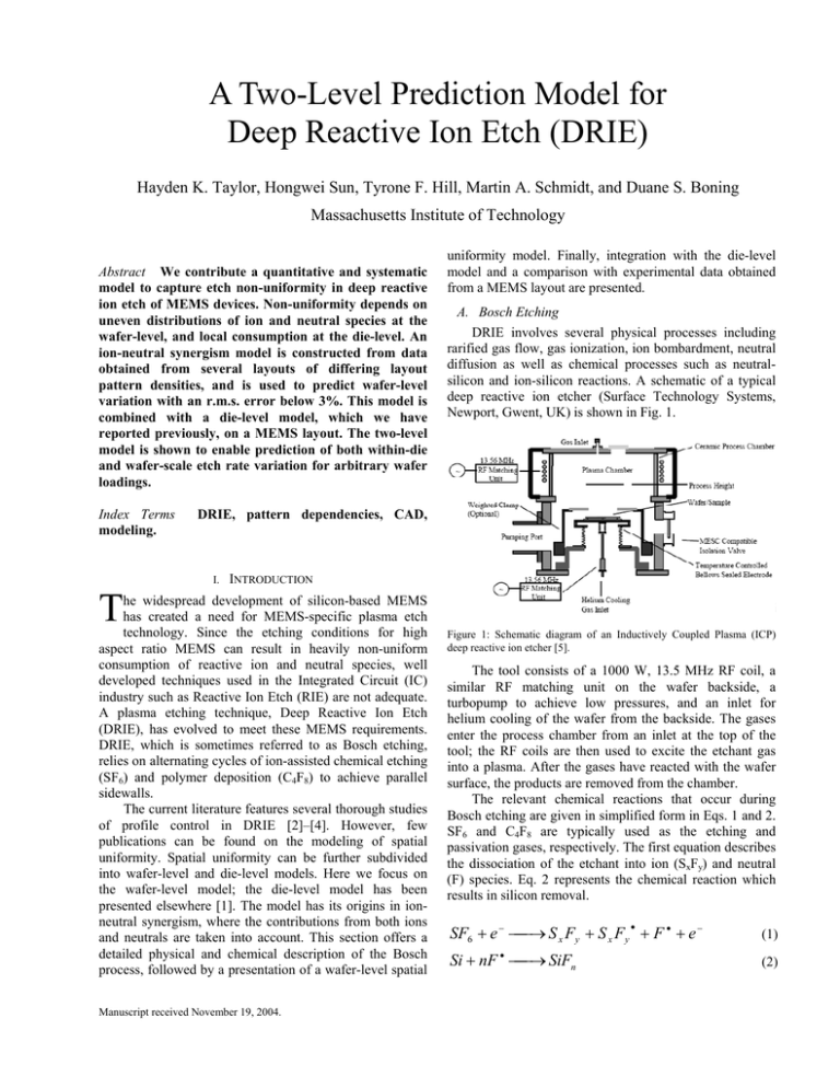
diffusion as well as chemical processes such as neutralsilicon and ion-silicon reactions. A schematic of a typical
deep reactive ion etcher (Surface Technology Systems,
Newport, Gwent, UK) is shown in Fig. 1.
DRIE, pattern dependencies, CAD,
I.
INTRODUCTION
T
he widespread development of silicon-based MEMS
has created a need for MEMS-specific plasma etch
technology. Since the etching conditions for high
aspect ratio MEMS can result in heavily non-uniform
consumption of reactive ion and neutral species, well
developed techniques used in the Integrated Circuit (IC)
industry such as Reactive Ion Etch (RIE) are not adequate.
A plasma etching technique, Deep Reactive Ion Etch
(DRIE), has evolved to meet these MEMS requirements.
DRIE, which is sometimes referred to as Bosch etching,
relies on alternating cycles of ion-assisted chemical etching
(SF6) and polymer deposition (C4F8) to achieve parallel
sidewalls.
The current literature features several thorough studies
of profile control in DRIE [2]–[4]. However, few
publications can be found on the modeling of spatial
uniformity. Spatial uniformity can be further subdivided
into wafer-level and die-level models. Here we focus on
the wafer-level model; the die-level model has been
presented elsewhere [1]. The model has its origins in ionneutral synergism, where the contributions from both ions
and neutrals are taken into account. This section offers a
detailed physical and chemical description of the Bosch
process, followed by a presentation of a wafer-level spatial
Manuscript received November 19, 2004.
Figure 1: Schematic diagram of an Inductively Coupled Plasma (ICP)
deep reactive ion etcher [5].
The tool consists of a 1000 W, 13.5 MHz RF coil, a
similar RF matching unit on the wafer backside, a
turbopump to achieve low pressures, and an inlet for
helium cooling of the wafer from the backside. The gases
enter the process chamber from an inlet at the top of the
tool; the RF coils are then used to excite the etchant gas
into a plasma. After the gases have reacted with the wafer
surface, the products are removed from the chamber.
The relevant chemical reactions that occur during
Bosch etching are given in simplified form in Eqs. 1 and 2.
SF6 and C4F8 are typically used as the etching and
passivation gases, respectively. The first equation describes
the dissociation of the etchant into ion (SxFy) and neutral
(F) species. Eq. 2 represents the chemical reaction which
results in silicon removal.
•
SF6 + e − ⎯
⎯→ S x Fy + S x Fy + F • + e −
(1)
Si + nF • ⎯
⎯→ SiFn
(2)
High aspect ratio directional etching is achieved by
alternating between etching and passivation cycles. In the
first step, a thin polymeric layer of CF2 is deposited over a
feature. Next, ions accelerated in the plasma sheath remove
the polymer from the feature bottom, which is then
chemically etched by the fluorine radicals in synergy with
energetic ion interactions. Both steps typically range
between 5 and 12 seconds in length. Gottscho et al.
developed an ion–neutral synergism model [6] of the
contributions of both ions and neutrals to the etch cycle:
1
1
1
=
+
R kE i J i vS o J n
(3)
where R is the etch rate, k and v represent the volume of
silicon removed by per unit ion bombardment energy and
reacting neutral respectively, Ji and Jn are the ion and
neutral fluxes to the surface, Ei is the ion energy, and S0 is
the sticking probability of neutrals to the wafer surface. In
general, uniformity depends on several parameters,
including ion density, neutral density, and ionic energy at
various locations across the wafer, and wafer temperature
[7].
In our preliminary work, a wafer-level spatial
uniformity map was assumed to be identical to one of a
series of etch maps with loading ranging from 0.1% to
17.6%. Loading is defined as the ratio of etchable area to
wafer area. The assumption underlying this method is that
the wafer-level uniformity will remain approximately the
same for nearby values of overall etch loading. For
example, a wafer map representing 1.2% loading might be
used on a layout with 3% loading. The goal of the new
model reported below is to enable intelligent interpolation
across the different uniformity maps empirically observed,
so that wafer-level uniformity can be accurately predicted
for any wafer loading fraction across both ion-dominated
and neutral-dominated regimes.
II. THEORY AND METHOD
As is outlined in Eq. 3, the ion-neutral synergism
model contains contributions from both the ion and neutral
fluxes. The ion flux distribution across the wafer depends
on asymmetries in the chamber setup; it is believed to be
relatively consistent, independent of the overall loading of
a layout. Thus, we begin by considering only the neutral
distribution across the wafer. An expression for species
conservation just above the wafer surface is given in Eq. 4:
∂C j
∂t
= D∇ 2 C j + G j − R j
(4)
where Cj is our species of interest (monatomic fluorine), D
is the diffusivity of monatomic fluorine, Gj is the
generation rate of monatomic fluorine, and Rj the decay of
reactive fluorine into diatomic fluorine (F2). Several
authors have explored analytical and numerical solutions
for this differential equation [7]; we are more concerned
with empirically modeling its parameters than determining
a closed-form solution. In the development of the wafer
level model we neglect lateral diffusion across the wafer;
thus the diffusive term in eliminated. Lateral interactions
between features are addressed by the die-level model.
Assuming a steady state situation, we can more explicitly
define a relation between the generation and consumption
rates:
Cj
G j − α 1 [ϕ + α 2 (1 − ϕ )]C j −
τ
=0
(5)
Here τ is the average neutral lifetime [s], φ is the
proportion of the region in which the silicon is exposed, α1
is a constant [s–1] for the tool and etch recipe relating the
consumption of neutrals to their concentration, and α2 is a
dimensionless constant reflecting neutrals’ selectivity of Si
over oxide in DRIE. Rearranging Eq. 4 gives
Cj =
G jτ
α 1τ [ϕ + α 2 (1 − ϕ )] + 1
(6)
In substituting for the vertical neutral flux, Jn, in the
ion-neutral synergism model, we must substitute an
expression for the flux at positions where silicon is
exposed, rather than an expression for the average flux
over exposed and unexposed silicon. Only neutrals that
stick to the silicon surface can react, and hence we may
write
S 0 J n , j = α1 H C j
(7)
where S0 is the sticking probability of neutrals to exposed
bare silicon sites, Jn,j is the downwards neutral flux just
above the wafer at any part of region j that sees exposed
silicon, and H is a characteristic height of the dark field
above the wafer surface. It is probable that α1H will be
approximately equal in magnitude to the r.m.s. speed of
neutrals in the chamber.
Substituting for S0Jn,j into the synergism model gives
the etch rate Rj for each region as:
Rj =
(kE J )(vα HG τ )
(vα HG τ ) + (kE J ){α τ [ϕ + α (1 − ϕ )] + 1}
i
1
j
i, j
i
i, j
1
1
j
(8)
2
A. Model Extraction and Simulation
We are aiming to predict the silicon etch rate at any
position j in the etch chamber for any value of loading, φ.
Theory leads to the idea that, in order to make such
predictions, we first need to estimate two tool-specific
maps: one describing how ion flux varies across the
chamber, and another describing how the generation rate of
fluorine neutrals varies with position. We also need to
estimate the two scalar constants α1τ and α2 to characterize
the process.
To obtain enough data to estimate these maps and
constants, we etched three wafers with different amounts of
F=
A j (i )B j (i )
B j (i ) + A j (i ){α 1τ [ϕ + α 2 (1 − ϕ )] + 1}
(10)
i
1 2 3 4 5 6 7 8 9
x location /16mm
1 2 3 4 5 6 7 8 9
x location /16mm
Simulated, 1.1%
Simulated, 4.4%
1
2
3
4
5
6
7
8
9
y location /16mm
y location /16mm
1 2 3 4 5 6 7 8 9
x location /16mm
1
2
3
4
5
6
7
8
9
1 2 3 4 5 6 7 8 9
x location /16mm
1 2 3 4 5 6 7 8 9
x location /16mm
Simulated, 17.6%
1
2
3
4
5
6
7
8
9
y location /16mm
Simulated, 0.1%
1
2
3
4
5
6
7
8
9
Measured, 17.6%
1
2
3
4
5
6
7
8
9
y location /16mm
y location /16mm
y location /16mm
y location /16mm
1 2 3 4 5 6 7 8 9
x location /16mm
Measured, 4.4%
1
2
3
4
5
6
7
8
9
1
2
3
4
5
6
7
8
9
1 2 3 4 5 6 7 8 9
x location /16mm
1 2 3 4 5 6 7 8 9
x location /16mm
Figure 2: Comparison of experimental and modeled etch rates for four
global wafer loadings.
4.2
1.1% loading
0.1% loading
4.0
(9)
192
∑F
Measured, 1.1%
Measured, 0.1%
1
2
3
4
5
6
7
8
9
i =1
We initially assumed α2 to be 0.01, reflecting the
approximate selectivity of Si over the oxide mask in DRIE.
Initial guesses for A, B and α1τ were calculated by
assuming all elements of A and B to be equal. An iterative
non-linear least-squares solution of the 192 simultaneous
equations given by the experimental data was performed in
MatLab. The extracted constants were then used to predict
etch rates across a wafer with 4.4% of its surface exposed,
and the predictions were compared to measured etch rates
from a fourth experimental wafer, featuring 4.4% loading
and processed in the manner already described.
Silicon etch rate (m s−1 × 10⁻⁸)
Fi = Ri −
underestimate the magnitude of the etch rates at 4.4%
loading, although with a relatively small r.m.s. error of
2.6%.
y location /16mm
exposed silicon and determined silicon etch rates on those
wafers as a function of position. The oxide masking layer
on each of three 150 mm-diameter silicon wafers was
patterned with a grid of circular openings, the number and
diameter of which determined the loading, φ. Wafers were
prepared with opening densities of 0.1%, 1.1% and 17.6%.
Each wafer was etched in turn for 30 minutes using the
following recipe: 105 sccm SF6 for 14 s at 25 mtorr (100
W platen power and 750 W coil power) interspersed with
40 sccm of C4F8 for 11 s at 12 mtorr (60 W platen power
and 600 W coil power). On each wafer the depths of 64 of
the etched circular holes, on a 16 mm-pitch square grid,
were measured interferometrically.
From the data obtained, two 64-point maps and two
scalar constants were extracted. In Eq. 9 below, kEiJi,j = Aj
[ms–1] and vα1HGjτ = Bj [ms–1]. F is the objective function
minimized in order to arrive at our estimates. Each of the
192 test locations, i, on the three characterization wafers
corresponds to one of the 64 chamber locations j, and
yields a contribution Fi to the objective function:
3.8
3.6
3.4
4.4% loading
(simulation)
4.4% loading
(measured)
3.2
17.6% loading
3.0
2.8
2.6
0
10
20
30
40
50
60
Location in chamber, ’snaking’ from top to bottom
Measurement Indices
1
1
2
8
7
6
5
4
3
9
10
11
12
13
14
15
16
25
24
23
22
21
20
19
18
17
26
27
28
29
30
31
32
33
34
43
42
41
40
39
38
37
36
35
44
45
46
47
48
49
50
51
52
59
58
57
56
55
54
53
60
61
62
63
64
2
3
III. RESULTS AND DISCUSSION
Fig. 2 illustrates etch rate predictions, made using the
extracted ion and neutral density maps, next to the
corresponding experimental data. Fig. 3 plots measured
and predicted etch rates where the horizontal axis
corresponds to a “snaking” path around each wafer, as
illustrated in Fig. 4. Figs. 2 and 3 confirm that the leastsquares fitting procedure has successfully matched our
model to the data. In the case of the 4.4% loading
previously “unseen” by the model, our approach
successfully predicts the way in which etch rates vary
across the wafer. As loading increases, an evolution is seen
in the form of this variation. At lower loading percentages,
we see a “hot spot” of faster etching, while the 17.6% data
is defined by a “cold spot” of slower etching. This
evolution is illustrated further in Fig. 4. The location of the
“hot spot” coincides approximately with the center of the
tool’s plasma-generating coil. The model does, however,
4
5
6
7
8
9
10
1
2
3
4
5
6
7
8
9
10
Figure 3: Evolution of etch profile from 0.1% to 17.6% loading,
“snaking” from top to bottom. The model was fit to the 0.1%, 1.1%, and
17.6% maps. Measurement indices are given in the lower diagram.
−8
4.2
1% loading
x 10
increasing loading
4
4.0
experiment series B
experiment series A
3.8
Silicon etch rate (m s−1)
Silicon etch rate (m s−1 × 10⁻⁸)
3.5
3.6
3.4
3.2
predictions based on series A
3
predictions based on series B
2.5
2
1.5
3.0
1
2.8
19% loading
2.6
0
10
20
30
40
50
Location in chamber, ’snaking’ from top to bottom
60
Figure 4: The evolution of wafer-scale etch non-uniformity as the total
exposed area of silicon is increased. At 1% loading, the non-uniformity is
characterized by a ‘hot spot’ of particularly rapid etching on the left hand
side of the wafer; at 19% loading, the non-uniformity is better described
by a ‘cold spot’ of slower etching on the right. Chamber locations are as
given in Fig. 3.
We have also tested our modeling approach on a
second data set, which was obtained in a similar way using
the same etching machine a year later. For this second data
set, wafers were etched with opening densities of 0.1%,
4.4%, 7.3% and 99.9%. The parameters of our model were
fitted to the data obtained at loadings of 0.1%, 4.4% and
99.9%. Data obtained at 7.3% loading were used as an
“unseen” set with which to test the model. The
interferometric measurements of etch depths made from the
wafer with 7.3% loading were on a grid of a different pitch
from that of the other data, and so linear interpolation was
used to calculate a set of etch rates for easy comparison.
Our model, together with the newly extracted parameters,
predicted etch rates at 7.3% loading with an r.m.s. error of
4.5%.
Fig. 5 collates all the data obtained and compares etch
rate predictions based on data sets A (taken in 2001) and B
(taken in 2002). The graph reiterates that as the amount of
exposed silicon increases, the average silicon etch rate
falls. It is also apparent that as loading increases, the
variation of silicon etch rate across the wafer becomes
greater.
The etch rate predictions based on data sets A and B
are of a similar form, but, for any given loading, data set A
implies up to 50% less variation in etch rate across the
wafer.
Future work should seek to examine etch rates for
loadings between 17.6% and 99.9%, and to investigate the
ways in which a particular etching machine’s wafer-level
non-uniformity changes over time.
0.5
0
10
20
30
40
50
60
70
80
Proportion of wafer exposed for etching (%)
90
100
Figure 5: Measured and predicted etch rates as a function of the proportion
of the wafer exposed for etching. Both data sets, and the predictions
extracted from them, are plotted in this figure. At any given value of
loading, a range of etch rates is observed across a wafer. The heights of
the vertical bars in this figure indicate the size of that range. The thick
vertical bars indicate the measured data; the bands constructed from thin
lines indicate predictions of etch rates made using parameters extracted
from the measured data.
A. Combining Predictions with Die-Level Perturbations
Our approach to wafer-scale etch rate variations assumes
that each of the wafer locations is equally loaded (i.e., the
etching pattern density is uniformly distributed across the
surface of the wafer). Central to our ability to model die-todie effects, however, is the inclusion of the diffusion of
reactants parallel to the wafer surface, which thereby
results in spatial non-uniformities due to localized
differences in the layout pattern density. The new waferlevel model can be combined with our die-level pattern
density model to predict uniformity for arbitrary layouts.
We assume the relationship between die-level and waferlevel effects is additive; exploration of other coupling
mechanisms is ongoing.
We demonstrate the combination of wafer and dielevel effects with a compressor blade layout from the MIT
microengine project. The layout, shown in Fig. 5, consists
of four dies with 42 mm spacing. An image of the layout is
given in Fig. 6, while Fig. 7 shows the prediction of
normalized etch rate for the lower left die. The
measurement was taken at an 8 mm radius from the center,
as is indicated by the dashed ring in Fig. 6.
V. ACKNOWLEDGMENTS
This paper is based on Ref. [16], which is to be
presented at MEMS ’05 in Miami, FL. This work has been
supported in part by the Singapore-MIT Alliance (SMA)
and by the Cambridge-MIT Institute (CMI). We also thank
Praesagus, Inc. for assistance with layout extractions.
42 mm
VI. REFERENCES
[1]
10 1
[2]
[3]
2 (position)
9
3
[4]
[5]
8
4
7
6
5
Figure 6: Close-up of compressor die layout; the measurements points are
indicated by the dashed ring. The actual layout size is 150 mm × 150 mm.
[6]
[7]
[8]
[9]
[10]
Model vs. Experimental Data (Die 3)
Normalized Etch Rate (dimensionless)
1.005
model
measured
[11]
1
[12]
0.995
[13]
0.99
[14]
[15]
[16]
0.985
0.98
0.975
1
2
3
4
5
6
7
8
9
10
position
Figure 7: Comparison between model and experimental data for the lower
left die in Fig. 4. The agreement indicates that the model is able to
accurately capture die-level pattern density effects.
IV. CONCLUSIONS
An ion-neutral synergism approach is used to model
the wafer-scale non-uniformity in the etching process of
DRIE. The model can be extracted from a simple set of
wafer-scale etch experiments, enabling identification of
both ion and neutral components of spatial non-uniformity.
The model can then predict the etch rate uniformity for
different wafer loadings. Our model can predict, within
less than 3% error on average, the wafer-scale variation of
etch rates for an arbitrary amount of exposed silicon on the
wafer. Finally, the model was successfully integrated with
our pattern density model and demonstrated on a MEMS
layout.
T. Hill et al., in Tech. Digest of 2002 Hilton Head Solid State
Sensors and Actuators Workshop, Hilton Head Island, SC (2004).
A. A. Ayon et al., J. of Electrochem. Soc., 146, 339 (1999).
J. Yeom et al., in 12th Int. Conf. On Solid State Sensors, Actuators,
and Microsystems, p. 1631, Boston, MA (2003).
J. Kiihamaki et al., JVST, A, 18, 2280 (2000).
J. Bhardwaj et al., “Dry Silicon Etching for MEMS,” Annual
Meeting of the Electrochemical Society, Montreal, Quebec, Canada,
May 1997.
R. A. Gottscho et al., JVST B, 10, 2133 (1992).
B. Andersen et al., JVST B, 15(4) (1997).
S. Yun et al., J. of App. Phys., 89, 911 (2001).
J. Karttunen et al., Proceedings of SPIE: Micromachining and
Microfabrication Process Technology VI, p. 90 (2000).
H. Ashraf et al., “Defining Conditions for the etching of silicon in
inductive coupled plasma reactor” in 1999 Materials Research
Society Fall Meeting, Boston, MA (1999).
H. Sun, T. Hill, M. A. Schmidt, and D. Boning, in 2003 Materials
Research Society Fall Meeting, Boston, MA (2003).
S. Shannon, J. Holloway, and M. L. Brake, JVST A, 17, 2703
(1999).
B.A. Andersen, O. Hansen, and M. Kristensen, JVST B, 15, 993
(1997).
M. D. Kilgore, H. M. Wu and D. B. Graves, JVST B, 12, 494 (1994).
A. H. Epstein et al., in 28th AIAA Fluid Dynamics Conf., Paper 97–
7113 (1997).
H. Sun et al., in 18th IEEE Int. Conf. MEMS (2005).
