MicroelectronicFab - ME EN 282 Manufacturing Processes
advertisement
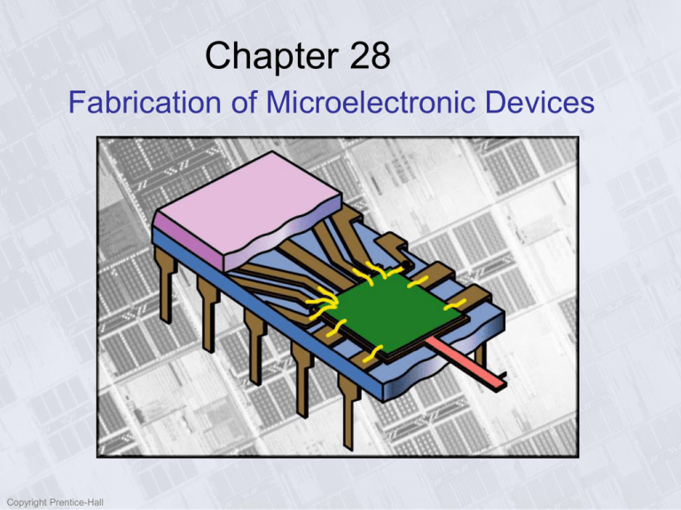
Chapter 28
Fabrication of Microelectronic Devices
Copyright Prentice-Hall
Parts Made by Chapter 28 Processes
(a)
(b)
(c)
Q18.2 (25) Point out the ball grid array in Figure 28.1.
(a) A completed eight-inch wafer with completed dice. (b) A single chip in a ballgrid array (BGA) with cover removed. (c) A printed circuit board. Source:
Courtesy of Intel Corporation.
Fabrication of
Integrated Circuits
Outline of the general fabrication
sequence for integrated circuits.
Fabrication of MOS
(metal-oxide semiconductor) Transistor
Cross-sectional views of the fabrication of a MOS transistor. Source:
After R. C. Jaeger.
Allowable Particle Size Counts for Clean Rooms
Allowable particle size counts for different clean room classes.
Crystallographic Structure and Miller Indices for Silicon
Crystallographic structure and Miller indices for silicon. (a) Construction of a diamond-type lattice
from interpenetrating face-centered cubic-cells; one of eight penetrating cells is shown. (b)
Diamond-type lattice of silicon; the interior atoms have been shaded darker than the surface atoms.
(c) Miller indices for a cubic lattice.
Finishing Operations on a
Silicon Ingot to Produce
Wafers
Finishing operations on a silicon ingot to
produce wafers (a) sawing the ends off
the ingot; (b) grinding of the end and
cylindrical surfaces of a silicon ingot; (c)
machining of a notch or flat; (d) slicing
of wafers; (e) end grinding of wafers; (f)
chemical-mechanical polishing of
wafers.
CVD Diagrams
Schematic diagrams of (a) a continuous, atmospheric-pressure CVD reactor
and (b) a low-pressure CVD. Source: After S. M. Sze.
Silicon Dioxide Growth
Growth of silicon dioxide showing consumption of silicon. Source:
After S. M. Sze.
General Characteristics of Lithography Techniques
Comparison of lithography techniques.
Spinning of Organic Coating on Wafer
Spinning of an organic coating on a wafer.
Techniques of Pattern Transfer
Schematic illustration of (a) wafer stepper technique to pattern
transfer and (b) step-and-scan technique.
Pattern Transfer by Photolithography
Pattern transfer by photolithography. Note that the mask in Step 3 can be a
positive or negative image of the pattern.
Moore’s Law
Illustration of Moore’s law. Source: After M. Madou.
Etching Directionality
Etching directionality. (a) Isotropic etching: etch proceeds vertically and horizontally
at approximately the same rate, with significant mask undercut. (b) Orientationdependant etching (ODE): etch proceeds vertically, terminating on {111} crystal
planes with little mask undercut. (c) Vertical etching: etch proceed vertically with
little mask undercut. Source: Courtesy of K. R. Williams, Agilent Laboratories.
Application of Boron Etch Stop and Back Etching
to Form Membrane and Orifice
Application of a boron etch stop and back etching to form a membrane and
orifice. Source: After Brodie, I., and Murray, J.J., The Physics of
Microfabrication, Plenum Press, 1982.
Machining Profiles Associated with Dry-Etching
Machining profiles associated with different dry-etching techniques: (a) sputtering;
(b) chemical; (c) ion-enhanced energetic; (d) ion-enhanced inhibitor. Source: After
M Madou.
Holes Generated from Square Mask
Various holes generated from a square mask in: (a) isotropic (wet) etching; (b)
orientation-dependant etching (ODE); (c) ODE with a larger hole; (d) ODE with a
rectangular hole; (e) deep reactive-ion etching; and (f) vertical etching. Source:
After M. Madou.
Interconnection of Integrated Circuit Hierarchy
Connections between elements in the hierarchy for integrated circuits.
Two-Level Metal Interconnect Structures
(a) Scanning electron microscope (SEM) photograph of a two-level metal interconnect.
Note the varying surface topography. (b) Schematic illustration of a two-level metal
interconnect structure. Source: (a) Courtesy of National Semiconductor Corporation. (b)
After R. C. Jaeger.
Wire Bonds Connecting Package Leads to
Die Bonding Pads
(a)
(b)
(c)
(a) SEM photograph of wire bonds connecting package leads (lefthand side) to die bonding pads. (b) and (c) Detailed views of (a).
Source: Courtesy of Micron Technology, Inc.
Thermosonic Welding of Gold Wires
Schematic illustration of thermosonic welding of gold wires from
package leads to bonding pads.
IC Packages
Schematic illustration of various IC packages: (a) dual-in-line
package (DIP); (b) flat, ceramic package; (c) common surface-mount
configurations; (d) ball-grid arrays.
Circuit Board Structures and Features
Printed circuit board structures and design features.
![Free-standing Al[subscript x]Ga[subscript 1x]As heterostructures by gas-phase etching of germanium Please share](http://s2.studylib.net/store/data/012057216_1-a9a188bc3b172f4312df083ff2cd104f-300x300.png)