SI232 ADMIN
advertisement
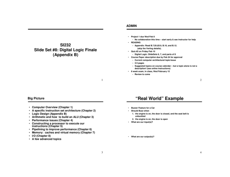
ADMIN • • SI232 Slide Set #8: Digital Logic Finale (Appendix B) • • • Project 1 due Wed Feb 8 – No collaboration this time – start early & see instructor for help READING – Appendix: Read B.7,B.8,B.9, B.10, and B.12. (skip the Verilog details). Quiz #2 on Friday Feb 10 – Digital Logic: SlideSets 6, 7, and parts of 8 Course Paper description due by Feb 24 for approval – Current computer architectural topic/issue – 3-5 pages – Suggested topics on course calendar – but a topic alone is not a description! (see online instructions) 6 week exam, in class, Wed February 15 – Review to come 1 2 “Real World” Example Big Picture • • • • • • • • • • Computer Overview (Chapter 1) A specific instruction set architecture (Chapter 2) Logic Design (Appendix B) Arithmetic and how to build an ALU (Chapter 3) Performance issues (Chapter 4) Constructing a processor to execute our instructions (Chapter 5) Pipelining to improve performance (Chapter 6) Memory: caches and virtual memory (Chapter 7) I/O (Chapter 8) A few advanced topics • • 3 • Buzzer Feature for a Car Should Buzz when 1. the engine is on, the door is closed, and the seat belt is unbuckled 2. the engine is on, the door is open What are our input(s)? • What are our output(s)? 4 (extra space) Check Yourself • • • • Could you have filled in the truth table? Could you have filled in the K-Map? Can you use the K-Map to minimize the equation? Can you draw the circuit? 6 Bigger Units of Combinational Logic • • Multiplexor – Example Usage Gates useful but fairly low level Easier to constructs circuits with higher-level building blocks instead: – Combinational Logic $t0 $t1 $t2 • Multiplexors (mux) • Decoders – (later) Sequential Logic Adder • Registers • Arithmetic unit (ALU) • What is this an example of? $a2 $a3 7 8 Multiplexor – 1-bit version Multiplexor – Wider version EN • 32 bit wide, 2-way Mux: • Pictures don’t always show the width (especially if 32 bits) S1 S0 D3 D2 D1 D0 • • • • Q Think of a mux as a selector S selects one input to be the output N-way mux has – # inputs: – # selector lines (S): – # outputs: Implementation? 9 Decoders 10 Decoder Implementation EN OR S2 S1 S0 x Q7 Q6 Q5 Q4 Q3 Q2 Q1 Q0 1 0 1 XY y 1 0 0 X~Y • • • Translates an n-bit input into a single asserted output – # inputs: – # outputs Named by inputs/outputs: Example uses: – Memory addressing – Identifying instruction op codes s1 s0 Q3 Q2 Q1 Q0 0 0 0 0 0 0 1 ~XY 0 1 0 0 1 0 1 0 0 1 0 0 0 0 ~X~Y 1 11 1 1 0 0 12 Exercise #1 • A. A 8-way mux has ______ “inputs” , _____ selector bit(s), and ______ output(s) • B. For a 3-input decoder, there are _______ output(s) • C. For a 4-input decoder, there are _______ output(s) Exercise #2 • Draw an 8-input mux with inputs: A, B, C, D, E, F, G, H and output: OUT (Remember to draw the selector bits) (you don’t need to draw the internals, just the external view) 13 Exercise #3 • 14 Implementing Combinational Logic Draw the internals of a 1 to 2 decoder. Given logic with inputs A, B, C; outputs D, E, F Several ways to implement combinational logic besides raw gates: 1. Read only memory 2. PLA (programmable logic arrays – next slide) Specific logic may be hardcoded at factory or programmable in field, depending on the technology 15 16 PLAs End of Combinational Logic 17 Combinational vs. Sequential Logic • Combinational Logic – output depends only on • Sequential Logic – output depends on: 18 Clocks and State Elements • • Clock Frequency is the __________ of _______________. When should updates occur to state elements? – Edge – change state when – Level – change state when • Previous inputs are stored in “state elements” – __________ determines when an element is updated • State elements will involve use of feedback in circuit – Not permitted in combinational circuits 19 20 Outline: Types of Memory Elements #1: S-R Memory Element • 1. Unclocked – Our example: S-R Memory Element – Our purpose: demonstrate feedback 2. Latches • Memory elements that are • Our example: D-type Latch • Our purpose: building block for flip-flops 3. Flip-Flops • Memory elements that are • Our example: D-type Flip-flop • Our purpose: Used extensively in CPU Output Q is the “state” of the latch Note: S-R element sometimes called S-R latch, but for this class we assumes all latches are clocked 21 Truth Tables Next State Tables S R 1 0 0 1 0 0 1 1 Action 22 #2: D-Latch • New kind of input: • • • • New kind of output: – Each X can be either a 0 or 1 (helps with minimization) – But in actual circuit, will have some specific value – Applies to combination logic too S\RQ 00 01 11 10 0 0 1 0 0 1 1 1 x x 23 State only changes when Latch is “open” when clock is high Latch is “closed” when clock is low – During this time Q-Latch 24 #3: D-Type Flip Flop • State only changes • Otherwise… remembers previous state Abstraction: • Exercise #1 – Complete the timing diagram below D Latch – active high D FlipFlop – falling edge triggered D Q C Q-Latch Q-FlipFlop Q-flipflop 25 26 Exercise #3 Exercise #2 – Complete diagram – note different assumptions D Latch – active low D FlipFlop – rising edge triggered • Draw the circuit diagram for D flip-flop that is rising-edge triggered. You may use a D-latch as a building block. Could you do this without looking at your notes? Q-Latch Q-FlipFlop 27 28 Exercise #4 - Stretch • State Diagrams Draw the Next State Table for a D-latch, including the clock as one of the inputs. Reduce this function with a K-map. Do you get the same function as the circuit we drew for this latch? • State = Contents of memory • Diagrams are a tool to represent ALL transitions from one state to another – What causes state changes? • Example for D Latch: Q=0 29 Finite State Machines • • • Can use state diagrams to express more complex sequential logic. Example: Candy Machine – Inputs: N (nickel received), D (dime received) – Outputs: C (dispense candy), R (give refund) – Should dispense candy after 15 cents deposited, + refund if overpaid. Then await next customer. We’ll use Moore machine – output depends only on • What states do we need? 30 Example: Candy Machine 31 Q=1 Inputs: (N)ickel, (D)ime Outputs: (C)andy, (R)efund 32 Exercise #1 • • Draw a state diagram for the following next state function: How would you describe what input ‘A’ is accomplishing? Exercise #2 A Qt Qt+1 0 0 0 0 1 1 1 0 1 1 1 1 • John and Mary agree to play rock-paper-scissors to decide who has to pay for dinner. The overall winner will be whoever wins two rounds in a row. • Assume you have 6 inputs: – JR, JP, JS (only one true depending on if John plays rock, paper, or scissors) – MR, MP, MS • At each round, 1. If John and Mary play the same (both scissors, etc.), then the game returns to the initial state. 2. If either John or Mary has just won twice in a row, the next state should be a “Game over” state. 3. Otherwise, the next state should reflect who won the most recent round Your task: 1. How many different states do you need? 2. Draw the next state diagram for this game Of course: Rock beats scissors Paper beats rock Scissors beats paper 33 Extra space 34 Exercise #3 • 35 How you could you make the rock/papers/scissors machine function on just 4 inputs? Draw the next state table for this version of the game. Do you have any don’t cares? 36 Implementing Finite State Machines • • • Squares = Circles = We don’t always show the clock for registers/memory diagrams, but will be implicit FSM Example 37 Registers and Register Files Combining Combinational and Sequential Logic • • 38 Finite State Machine was our first example of this Two general patterns: 1. State Machine • Registers store data (bits) (i.e. have memory) – Each register = • Register files contain: – Set of registers – Logic for read/write • MIPS register file has how many registers? • How does it store data? • How does it know which register to access? 2. Pipeline • In either case, have important timing concerns – Output of combinational logic block may oscillate before settling – Clock cycle time must be long enough so combo-logic settles before the sequential logic (state) reads the new value – State elements ensure that combo-logic inputs remain stable 39 40 Register Files - Read • • Read: Input = _____________; Output = ________ How / why is the mux used? • What is the width (bits) of the output? Register Files - Write • • Write: Input = Output = How / why is the decoder used? • Why the clock? 41 Memory 42 Static Random Access Memory (SRAM) • Why so many types? • Basic types: – RAM “random access memory” (read/write) • Main memory • Volatile • Types: • • • • Relative expensive, fast memory – used for cache memory Usually just one port to read or write Height (15) / width (8) relationship What do we need for a write? • for a read? – SRAM – async, sync, pipeline burst, cache; – DRAM – M, FPM, EDO, burst EDO, sync, DR, DDR – ROM (read only) • • • • • Small Stores critical operating instruction (BOOT strap) Non-volatile Common in embedded system (toys, cameras, printers, etc) Types: PROM, EPROM, EEPROM, flash memory 43 44 Static Random Access Memory (SRAM) • On read ,how to select the proper data (register) for output? – i.e. which Flip-Flops have the data? – Register file uses mux – problem? • Solution: Shared output line (aka bit line) • Each flip-flop has “tri-state buffer” output – One asserted at a given time • Otherwise, can’t connect outputs together! Where does select signals come from? Dynamic Random Access Memory (DRAM) • • • • • • • • Each bit stored via charge in a capacitor Data accessed via a transistor – Single transistor per bit of storage (SRAM 4 to 6 per bit) – Dense and cheap Problem? Refresh – Via reading and writing contents back to cell – By rows vice individual cells – ~2 % of cycles needed (98% available for data read & write) 2 level decode structure – Part of address specifies “row” – Part of address specifies “column” – Access time 5 - 10x longer than SRAM Less expensive than SRAM Used in main memory 45 In the Book • • 46 Appendix B Summary • DRAM usage details Error correction – parity, error correcting codes • • • • • 47 Truth tables and Gates – AND, OR, NOT, NOR, NAND, XOR Boolean Algebra – Distributive, DeMorgan’s, Inverse, Identity, etc Combinational Logic – Circuits – Design, reduction / minimization, K-maps – Decoder & multiplexor Sequential Logic – Latches, Flip/flops – Clock & state diagrams Register files Memory – RAM vs ROM, SRAM vs. DRAM 48
