ISSCC 2001 / SESSION 10 / WIRELESS BUILDING BLOCKS I /... 10.4: A 1.75GHz Highly-Integrated Narrow-Band CMOS Transmitter with Harmonic-Rejection Mixers
advertisement
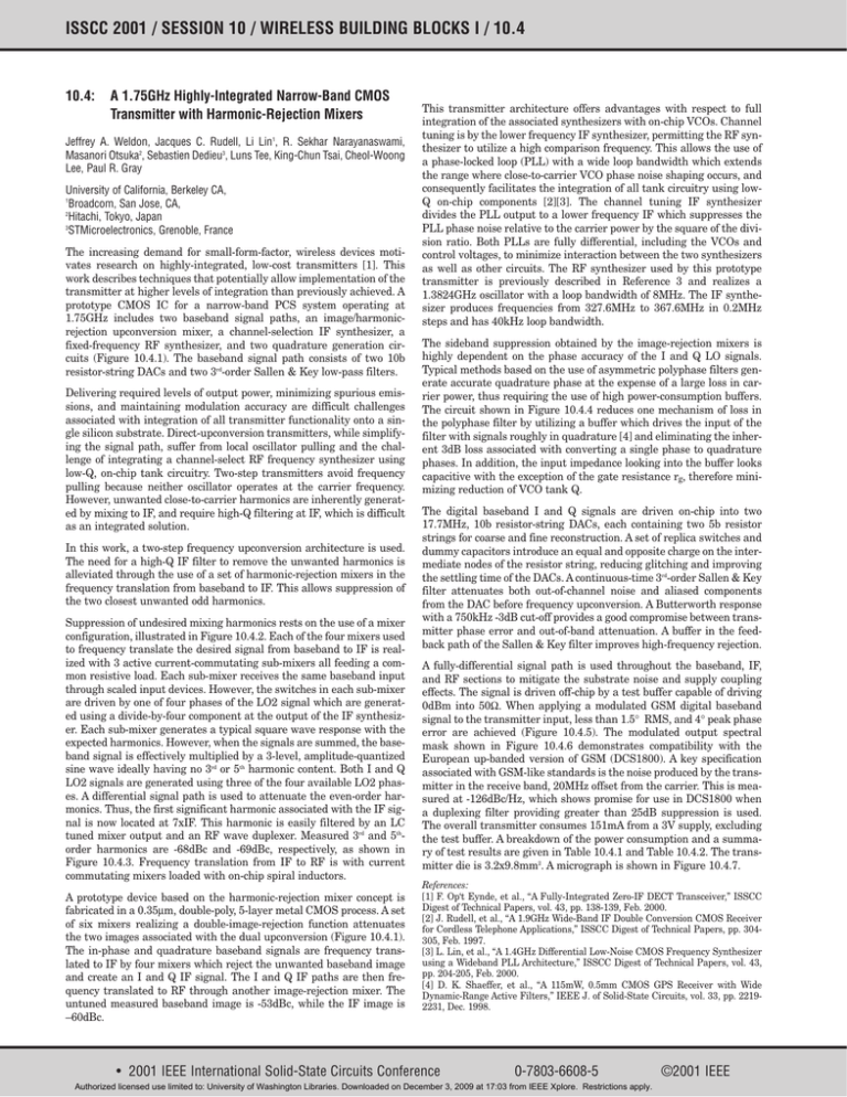
ISSCC 2001 / SESSION 10 / WIRELESS BUILDING BLOCKS I / 10.4 10.4: A 1.75GHz Highly-Integrated Narrow-Band CMOS Transmitter with Harmonic-Rejection Mixers Jeffrey A. Weldon, Jacques C. Rudell, Li Lin1, R. Sekhar Narayanaswami, Masanori Otsuka2, Sebastien Dedieu3, Luns Tee, King-Chun Tsai, Cheol-Woong Lee, Paul R. Gray University of California, Berkeley CA, 1 Broadcom, San Jose, CA, 2 Hitachi, Tokyo, Japan 3 STMicroelectronics, Grenoble, France The increasing demand for small-form-factor, wireless devices motivates research on highly-integrated, low-cost transmitters [1]. This work describes techniques that potentially allow implementation of the transmitter at higher levels of integration than previously achieved. A prototype CMOS IC for a narrow-band PCS system operating at 1.75GHz includes two baseband signal paths, an image/harmonicrejection upconversion mixer, a channel-selection IF synthesizer, a fixed-frequency RF synthesizer, and two quadrature generation circuits (Figure 10.4.1). The baseband signal path consists of two 10b resistor-string DACs and two 3rd-order Sallen & Key low-pass filters. Delivering required levels of output power, minimizing spurious emissions, and maintaining modulation accuracy are difficult challenges associated with integration of all transmitter functionality onto a single silicon substrate. Direct-upconversion transmitters, while simplifying the signal path, suffer from local oscillator pulling and the challenge of integrating a channel-select RF frequency synthesizer using low-Q, on-chip tank circuitry. Two-step transmitters avoid frequency pulling because neither oscillator operates at the carrier frequency. However, unwanted close-to-carrier harmonics are inherently generated by mixing to IF, and require high-Q filtering at IF, which is difficult as an integrated solution. In this work, a two-step frequency upconversion architecture is used. The need for a high-Q IF filter to remove the unwanted harmonics is alleviated through the use of a set of harmonic-rejection mixers in the frequency translation from baseband to IF. This allows suppression of the two closest unwanted odd harmonics. Suppression of undesired mixing harmonics rests on the use of a mixer configuration, illustrated in Figure 10.4.2. Each of the four mixers used to frequency translate the desired signal from baseband to IF is realized with 3 active current-commutating sub-mixers all feeding a common resistive load. Each sub-mixer receives the same baseband input through scaled input devices. However, the switches in each sub-mixer are driven by one of four phases of the LO2 signal which are generated using a divide-by-four component at the output of the IF synthesizer. Each sub-mixer generates a typical square wave response with the expected harmonics. However, when the signals are summed, the baseband signal is effectively multiplied by a 3-level, amplitude-quantized sine wave ideally having no 3rd or 5th harmonic content. Both I and Q LO2 signals are generated using three of the four available LO2 phases. A differential signal path is used to attenuate the even-order harmonics. Thus, the first significant harmonic associated with the IF signal is now located at 7xIF. This harmonic is easily filtered by an LC tuned mixer output and an RF wave duplexer. Measured 3rd and 5thorder harmonics are -68dBc and -69dBc, respectively, as shown in Figure 10.4.3. Frequency translation from IF to RF is with current commutating mixers loaded with on-chip spiral inductors. A prototype device based on the harmonic-rejection mixer concept is fabricated in a 0.35µm, double-poly, 5-layer metal CMOS process. A set of six mixers realizing a double-image-rejection function attenuates the two images associated with the dual upconversion (Figure 10.4.1). The in-phase and quadrature baseband signals are frequency translated to IF by four mixers which reject the unwanted baseband image and create an I and Q IF signal. The I and Q IF paths are then frequency translated to RF through another image-rejection mixer. The untuned measured baseband image is -53dBc, while the IF image is –60dBc. This transmitter architecture offers advantages with respect to full integration of the associated synthesizers with on-chip VCOs. Channel tuning is by the lower frequency IF synthesizer, permitting the RF synthesizer to utilize a high comparison frequency. This allows the use of a phase-locked loop (PLL) with a wide loop bandwidth which extends the range where close-to-carrier VCO phase noise shaping occurs, and consequently facilitates the integration of all tank circuitry using lowQ on-chip components [2][3]. The channel tuning IF synthesizer divides the PLL output to a lower frequency IF which suppresses the PLL phase noise relative to the carrier power by the square of the division ratio. Both PLLs are fully differential, including the VCOs and control voltages, to minimize interaction between the two synthesizers as well as other circuits. The RF synthesizer used by this prototype transmitter is previously described in Reference 3 and realizes a 1.3824GHz oscillator with a loop bandwidth of 8MHz. The IF synthesizer produces frequencies from 327.6MHz to 367.6MHz in 0.2MHz steps and has 40kHz loop bandwidth. The sideband suppression obtained by the image-rejection mixers is highly dependent on the phase accuracy of the I and Q LO signals. Typical methods based on the use of asymmetric polyphase filters generate accurate quadrature phase at the expense of a large loss in carrier power, thus requiring the use of high power-consumption buffers. The circuit shown in Figure 10.4.4 reduces one mechanism of loss in the polyphase filter by utilizing a buffer which drives the input of the filter with signals roughly in quadrature [4] and eliminating the inherent 3dB loss associated with converting a single phase to quadrature phases. In addition, the input impedance looking into the buffer looks capacitive with the exception of the gate resistance rg, therefore minimizing reduction of VCO tank Q. The digital baseband I and Q signals are driven on-chip into two 17.7MHz, 10b resistor-string DACs, each containing two 5b resistor strings for coarse and fine reconstruction. A set of replica switches and dummy capacitors introduce an equal and opposite charge on the intermediate nodes of the resistor string, reducing glitching and improving the settling time of the DACs. A continuous-time 3rd-order Sallen & Key filter attenuates both out-of-channel noise and aliased components from the DAC before frequency upconversion. A Butterworth response with a 750kHz -3dB cut-off provides a good compromise between transmitter phase error and out-of-band attenuation. A buffer in the feedback path of the Sallen & Key filter improves high-frequency rejection. A fully-differential signal path is used throughout the baseband, IF, and RF sections to mitigate the substrate noise and supply coupling effects. The signal is driven off-chip by a test buffer capable of driving 0dBm into 50Ω. When applying a modulated GSM digital baseband signal to the transmitter input, less than 1.5° RMS, and 4° peak phase error are achieved (Figure 10.4.5). The modulated output spectral mask shown in Figure 10.4.6 demonstrates compatibility with the European up-banded version of GSM (DCS1800). A key specification associated with GSM-like standards is the noise produced by the transmitter in the receive band, 20MHz offset from the carrier. This is measured at -126dBc/Hz, which shows promise for use in DCS1800 when a duplexing filter providing greater than 25dB suppression is used. The overall transmitter consumes 151mA from a 3V supply, excluding the test buffer. A breakdown of the power consumption and a summary of test results are given in Table 10.4.1 and Table 10.4.2. The transmitter die is 3.2x9.8mm2. A micrograph is shown in Figure 10.4.7. References: [1] F. Op‘t Eynde, et al., “A Fully-Integrated Zero-IF DECT Transceiver,” ISSCC Digest of Technical Papers, vol. 43, pp. 138-139, Feb. 2000. [2] J. Rudell, et al., “A 1.9GHz Wide-Band IF Double Conversion CMOS Receiver for Cordless Telephone Applications,” ISSCC Digest of Technical Papers, pp. 304305, Feb. 1997. [3] L. Lin, et al., “A 1.4GHz Differential Low-Noise CMOS Frequency Synthesizer using a Wideband PLL Architecture,” ISSCC Digest of Technical Papers, vol. 43, pp. 204-205, Feb. 2000. [4] D. K. Shaeffer, et al., “A 115mW, 0.5mm CMOS GPS Receiver with Wide Dynamic-Range Active Filters,” IEEE J. of Solid-State Circuits, vol. 33, pp. 22192231, Dec. 1998. • 2001 IEEE International Solid-State Circuits Conference 0-7803-6608-5 Authorized licensed use limited to: University of Washington Libraries. Downloaded on December 3, 2009 at 17:03 from IEEE Xplore. Restrictions apply. ©2001 IEEE ISSCC 2001 / February 6, 2001 / Salon 9 / 9:30 AM Figure 10.4.1: Harmonic-rejection transmitter system. Figure 10.4.2: Harmonic rejection mixer (HRM). Figure 10.4.3: Transmitter wide-band spurious emission. Figure 10.4.4: LO1 VCO buffer quadrature phase shifter with onchip spiral inductors L1 through L4. Figure 10.4.5: Results of GSM modulation accuracy test. Figure 10.4.6: Measured output spectrum with GSM modulation. • 2001 IEEE International Solid-State Circuits Conference 0-7803-6608-5 Authorized licensed use limited to: University of Washington Libraries. Downloaded on December 3, 2009 at 17:03 from IEEE Xplore. Restrictions apply. ©2001 IEEE Table 10.4.1: Transmitter current consumption. Single Sideband Suppression -53dBc LO2 3rd & 5th Harm. Reject. >-68dBc IF Image Suppression >-60dBc RF Carrier Suppression >-38dBc Phase error (RMS) 1.3O Phase error (peak) 3.7O 20MHz offset carrier noise -126dBc/Hz Third Order Distortation (IM3) -46dBc Table 10.4.2: Results summary. • 2001 IEEE International Solid-State Circuits Conference 0-7803-6608-5 Authorized licensed use limited to: University of Washington Libraries. Downloaded on December 3, 2009 at 17:03 from IEEE Xplore. Restrictions apply. ©2001 IEEE
