Single Chip Realizes Direct-Conversion Rx
advertisement
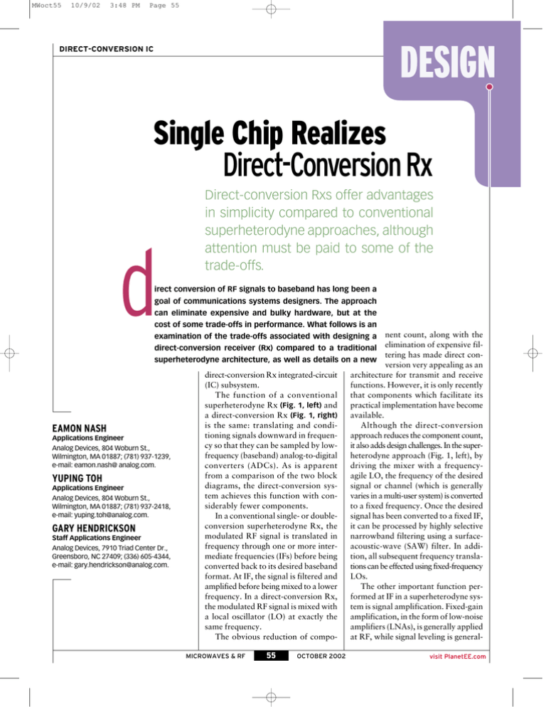
MWoct55 10/9/02 3:48 PM Page 55 DESIGN DIRECT-CONVERSION IC Single Chip Realizes Direct-Conversion Rx d Direct-conversion Rxs offer advantages in simplicity compared to conventional superheterodyne approaches, although attention must be paid to some of the trade-offs. irect conversion of RF signals to baseband has long been a goal of communications systems designers. The approach can eliminate expensive and bulky hardware, but at the cost of some trade-offs in performance. What follows is an nent count, along with the direct-conversion receiver (Rx) compared to a traditional elimination of expensive filtering has made direct consuperheterodyne architecture, as well as details on a new version very appealing as an direct-conversion Rx integrated-circuit architecture for transmit and receive (IC) subsystem. functions. However, it is only recently The function of a conventional that components which facilitate its superheterodyne Rx (Fig. 1, left) and practical implementation have become a direct-conversion Rx (Fig. 1, right) available. is the same: translating and condiAlthough the direct-conversion EAMON NASH tioning signals downward in frequenapproach reduces the component count, Applications Engineer cy so that they can be sampled by lowit also adds design challenges. In the superAnalog Devices, 804 Woburn St., frequency (baseband) analog-to-digital heterodyne approach (Fig. 1, left), by Wilmington, MA 01887; (781) 937-1239, e-mail: eamon.nash@ analog.com. converters (ADCs). As is apparent driving the mixer with a frequencyfrom a comparison of the two block agile LO, the frequency of the desired YUPING TOH diagrams, the direct-conversion syssignal or channel (which is generally Applications Engineer tem achieves this function with convaries in a multi-user system) is converted Analog Devices, 804 Woburn St., siderably fewer components. to a fixed frequency. Once the desired Wilmington, MA 01887; (781) 937-2418, e-mail: yuping.toh@analog.com. In a conventional single- or doublesignal has been converted to a fixed IF, conversion superheterodyne Rx, the it can be processed by highly selective GARY HENDRICKSON modulated RF signal is translated in narrowband filtering using a surfaceStaff Applications Engineer frequency through one or more interacoustic-wave (SAW) filter. In addiAnalog Devices, 7910 Triad Center Dr., Greensboro, NC 27409; (336) 605-4344, mediate frequencies (IFs) before being tion, all subsequent frequency translae-mail: gary.hendrickson@analog.com. converted back to its desired baseband tions can be effected using fixed-frequency format. At IF, the signal is filtered and LOs. amplified before being mixed to a lower The other important function perfrequency. In a direct-conversion Rx, formed at IF in a superheterodyne systhe modulated RF signal is mixed with tem is signal amplification. Fixed-gain a local oscillator (LO) at exactly the amplification, in the form of low-noise same frequency. amplifiers (LNAs), is generally applied The obvious reduction of compoat RF, while signal leveling is generalexamination of the trade-offs associated with designing a MICROWAVES & RF 55 OCTOBER 2002 visit PlanetEE.com MWoct56 10/9/02 3:48 PM Page 56 DESIGN IQ demod Splitter/ Combiner High-power amplifier AMP 0 90 VGA LNA ADC RSSI/ AGC Duplexer/ Switch VCO/Synth RF VGA DAC VGA Mixer RF power detection and control ADC ADC Mixer LNA IQ demod High-power amplifier 0 90 0 90 VGA ADC RSSI/ AGC VCO/Synth RF VGA DAC DAC IQ mod RF power detection and control 0 90 DAC IQ mod 1. A conventional single-conversion superheterodyne Rx translates the frequency of desired signals through one or more IFs before converting it to baseband. A direct-conversion Rx makes the transition directly from RF to baseband. ly accomplished through the use of variDevices (Norwood, MA). This Rx IC can imately 3 GHz), but they are generalable-gain amplifiers (VGAs). Since it demodulate signals from 0.8 to 2.7 ly more expensive than lower-frequency is easier to design a high-gain-range GHz. The device consists of a number IF filters due to the higher quality-facVGA at lower frequencies, and because of subcircuits that can be configured tor (Q) requirements. many unwanted signal components separately. The IC includes all of the A cost-effective means of realizing a have already been removed from the carcomponents required for amplification, direct-conversion Rx is through monorier by the time it is translated to IF, varidownconversion, and filtering in a directlithic fabrication, by including as many able-gain amplification is generally perconversion demodulation circuit. of the required components on a single formed at IF or baseband frequencies. Since gain control in a direct-conchip, such as the AD8347 direct-conThis “distribution” of gain avoids a version design must be implemented at version Rx IC (Fig. 2) from Analog concentration of high gain at the Rx’s front-end portion, VPS1 VPS2 VPS3 VREF IMXO IOFS IAIN IOPP IOPN which can cause saturation of 2 8 6 4 3 21 12 14 13 subsequent stages, especially VREF + if large in-band or out-of-band AD8347 signal blockers are present. – Bias ENBL 15 While the appeal of a direct5 VCMC cell VREF VCMO conversion Rx lies in its elimination of IF stages, therein Phase Phase 1 LOIN RFIN 10 splitter splitter lies its weakness. Because there 2 1 RFIP 11 28 LOIP is no longer an IF stage at which signal leveling and filVCMO 7 COM3 tering can be conveniently per2 pF + 9 COM2 formed, all signal conditionGainDET2 DET1 23 COM3 VREF ing must be performed either VGIN 17 control – interface 27 COM1 at RF or baseband. In a mul20 19 18 22 16 24 25 26 tichannel system, the capaQOPP QOPN VDT1 VAGC VDT2 QMXO QOFS QAIN bilities of RF filters are limited (they cannot be 2. The AD8347 is comprised of a 70-dB VGA with AGC mode, an I/Q demodulator and narrowband), at best screening out-oftwo 30-dB-gain baseband amplifiers. An internal +1-VDC voltage reference provides band interferers. SAW filters are availbiasing. able for some RF uses (through approxMICROWAVES & RF 56 OCTOBER 2002 p55,56,58,60,61,62,65,67 10/9/02 10/9/02 3:02 3:02PM PM Page Page Page58 58 58 (Black (Yellow (Cyan (Magenta plate) plate) plate) 45 40 35 30 25 20 15 10 5 0 –5 –10 –15 –20 –25 –30 –35 14 12 –40°C 10 +25°C 8 6 +85°C 4 +25°C 2 0 –2 +25°C –4 –40°C Linearity error—dB RF and/or at baseband, the AD8347 employs three stages of VGA. Two stages are employed at RF and one at baseband, following the I/Q demodulator. The three VGA stages, which have a convenient linear-in-dB gain-control relationship, are controlled in parallel. Each of the two RF VGAs has a gain range from –10 to +13 dB. The combined gain range of the mixer and the baseband VGA is –10 to +14 dBm. The overall gain range from the RF input to the mixer output is therefore –30 to +40 dB. The gain of the VGA is set by the voltage on the AD8347’s VGIN pin, which is a high-impedance input port. Figure 3 shows a plot of the gain versus gaincontrol voltage, along with the linearity of the gain-control function. Note that the sense of the gain-control voltage is negative. As the gain-control voltage increases from +0.2 to +1.2 VDC, the gain decreases from +40 to –30 dB. The VGA can be driven by an exter- Mixer gain—dB | DIRECT-CONVERSION IC | DESIGN –6 –8 –10 –12 0.2 0.3 0.4 0.5 0.6 0.7 0.8 Vgin—V 0.9 1.0 1.1 1.2 3. The three-stage VGA (two stages at RF, one stage at baseband) varies gain from –30 to +40 dB. The gain-control function is linear-in-dB over its range. nal voltage source [generally a digitalto-analog converter (DAC)] or by an automatic-gain-control (AGC) circuit built into the device. The AGC circuit con- sists of two root-mean-square (RMS) detectors and an error amplifier. When the AGC circuit is being used, the two mixer outputs are connected to the MWoct60 10/9/02 3:49 PM Page 60 DESIGN C1 4.7 pF RS 91 C3 8.2 pF L1 L3 0.68 H 1.2 H C2 150 pF C4 82 pF IMXO SYNTHESIZERS • VREF RL 100 IAIN VDT1 AD8347 4. The demodulated output (baseband-mixer output) can be filtered off-chip before being applied to the final baseband amplifiers. The on-chip reference voltage signal (VREF) provides biasing for the filter circuit. inputs of the two detectors. The signals (currents) from the detectors are compared with a set-point signal and an error signal is generated. The AGC circuit is completed by connecting the error signal to the Rx’s VGIN gain-control input pin. With the AGC circuit activated, the mixer’s output will remain constant for input levels from –55 to + 5 dBm. Because this output has a 90-MHz bandwidth, downconversion to a low IF is also possible. The mixer is a quadrature demodulator between the RF and baseband VGAs. It produces in-phase (I) and quadrature (Q) baseband outputs. To achieve low error-vector magnitude (EVM) in (direct-conversion) digital demodulation, precise quadrature splitting and amplitude balance of the LO signal is required. The AD8347 achieves typical phase and amplitude balances of 3 deg. and 0.3 dB, respectively, from 0.8 to 2.7 GHz. LO leakage within a direct-conversion system is one of the key challenges to implementing a high-sensitivity direct-conversion Rx. In direct-conversion and superheterodyne Rxs, some of the LO signal will leak through to the RF input. LO leakage to the RF input will cause self-mixing, which will produce a troublesome DC component at the mixer output. This DC component, if large enough, can lead to saturation of the baseband output signal (to either rail). In addition, because LO leakage is typically frequency dependent, the extent of the DC offset will also vary with frequency, making simple offset compensation difficult. In a conventional Rx, even if the first downconversion produces a DC component, this component will be harmless as it will be removed by IF filtering. This is an argument for using a direct-conversion Rx to mix the signal down to a low IF (instead of all the way to baseband) and digitizing those signals using IF sampling. The 90-MHz bandwidth of the AD8347’s mixer output easily facilitates this. The AD8347 uses two techniques to minimize the effects of LO leakage. First, the use of an active mixer means that the LO level can be set quite low. In the case of the AD8347, MICROWAVES & RF 60 OCTOBER 2002 MWoct61 10/9/02 3:49 PM Page 61 DESIGN the recommended level is –8 dBm. The device also contains a circuit that actively reduces DC offsets that appear at the output of the baseband VGA. Internally, the average level on the baseband outputs is compared to their nominal bias levels of +1 VDC. If there is any discrepancy between these two voltages, the average level at the mixer output is slowly servo-controlled back to +1 VDC. The settling time to this levelcorrecting circuit can be controlled through external capacitors. Because the output of the mixer/VGA circuit and the input to the final baseband amplifiers are separately pinned out, baseband lowpass or bandpass filtering can be conveniently performed before the signal faces its final amplification stage. The mixer/VGA output and the baseband amplifier inputs are biased to the same reference voltage level (of +1 VDC at VREF), making a DC-coupled connection permissible. Figure 4 shows a schematic diagram for a 100-Ω, fourth-order elliptic lowpass filter with a 3-dB cutoff of 20 MHz. Source and load impedances of approximately 100 Ω ensure that the filter experiences a matched source and load. This also ensures that the mixer output is driving an overall load of 200 Ω. Note that the shunt-termination resistor is tied to the reference voltage VREF and not to ground. The AD8347’s baseband amplifiers take single-ended input signals and boost them by 30 dB to produce a differential output which can be independently biased. The VOCM input pin, which sets the output common-mode level, can be driven by the AD8347’s internal +1VDC reference. Alternatively, the VOCM pin can be driven by an external reference voltage. In general, when the VOCM pin is driven externally, the drive voltage should come from the ADC that the AD8347 is driving. The differential outputs are capable of swinging from +0.4 VDC above ground to within +1.3 VDC of the supply voltage and have a 3-dB bandwidth of 65 MHz. Figure 5 shows a block diagram of a complete Rx signal chain that can be used to demodulate various signal types, 61 MWoct62 10/9/02 3:49 PM Page 62 | DIRECT-CONVERSION IC | DESIGN 5. A complete direct-conversion Rx can be assembled using the ADF4112, AD8347, and AD9218 ICs. including higher-order quadrature30-MHz frequency offset results. This able for rates of 40, 60, 80, and 100 amplitude-modulation (QAM) signals. 30-MHz offset (and including the freMSamples/s. The evaluation system includes the quency deviations of the modulation) The high-encode-rate capability and ADF4112 phase-locked loop (PLL), is well-within the 65-MHz bandwidth high analog bandwidth of the AD8347 with a range of 0.2 to 3 GHz, which easof the AD8347’s output amplifiers, as also make possible IF sampling appliily covers the 0.8-to-2.7-GHz LO range well as the analog bandwidth of the cations. By running a 1.9-GHz LO with of the AD8347. In this evaluation sysAD9218 ADC. The AD9218 successRF signals at 1.93 GHz, a (modulated) tem, a 1.9-GHz voltagefully mixed down these 30controlled oscillator (VCO) MHz offset signals to basewas used with the PLL, and band frequencies, showing a 1:1 balun was inserted the AD8347/AD9218 combetween the PLL and the bination to be suitable for AD8347’s LO input to prosome IF sampling applicavide a differential drive. tions. To evaluate the The I/Q outputs of the AD8347 as a direct-conAD8347, biased to the version Rx operating with AD8347’s internal refercomplex modulation, RF ence voltage, connect directinput signals to the AD8347 ly to the differential inputs were supplied from an of the AD9218 dual ADC. SMIQ-series vector-signal The AD9218 is a dual 10generator from Rohde & b device available for samSchwarz (Munich, Gerpling rates of 40, 65, 80, many). The instrument is and 105 MSamples/s (the capable of providing clean 105-MSamples/s version 1.9-GHz RF signals with a was used in this measurement variety of modulation forsetup). For lower-order modmats, including 16QAM ulation schemes, it is possible 6. Using a reconstruction DAC, the (digitized) demodulated constel- and 64QAM. to use the AD9288, a dual lation for a 2-MSymbol/s, 16-QAM signal can be displayed on a stanThe AD8347 and 8-b ADC with versions avail- dard oscilloscope screen. ADF4112 can operate at MICROWAVES & RF 62 OCTOBER 2002 MWoct65 10/9/02 3:50 PM Page 65 DESIGN supply voltages from +3 to +5 VDC. For the evaluation setup, a +3-VDC supply was used, matching the power-supply level of the AD9218. Baseband filtering prior to final output amplification (to improve performance through the elimination of out-of-band noise) is possible on the AD8347 evaluation board, but was not done during this evaluation. The AD8347’s VGA was set to run in AGC mode. In this mode, the mixer output settles to a level of approximately 24 mV peak to peak, resulting in a 760-mV peak-to-peak differential voltage at the baseband amplifier outputs. In addition to baseband lowpass filtering, the signal-to-noise ratio (SNR) of the demodulated signal can be With an input range from 0.8 to 2.7 GHz, the AD8347 is suitable for a broad range of markets. For systems operating beyond 2.7 GHz, it can also be used as an IF-tobaseband converter. improved by increasing the mixer output levels beyond this nominal 24-mV peak-to-peak level.1 The standard ADF4112 PLL printed-circuit board (PCB) is shipped with an 800-MHz external VCO. For this evaluation of the AD8347, the PLL module’s 800-MHz VCO was replaced with a 1.9-GHz VCO. Tuning of the AD4112’s output frequency was easily accomplished through the parallel port using a software package supplied with the PLL by Analog Devices. The PLL module’s PCB also features an onboard 10-MHz crystal-oscillator reference source, which was bypassed to allow for synchronization with external RF source (the SMIQ-series vector-signal generator). Before measurements could be made, the evaluation board for the AD9218 ADC required some modifications to enable common clocking and to meet 65 MWoct67 10/9/02 3:53 PM Page 67 DESIGN the limited drive capability of the clock source. The bit clock from the SMIQseries vector-signal generator supplied the required encode clock for the AD9218. For a 2-Msymbol/s data rate, this corresponded to an 8-MHz clock rate for 16QAM. The analog input 50Ω termination resistors on the PCB were switched to 1-kΩ terminations to accommodate the limited drive capability of the AD8347’s baseband output amplifiers. This resulted in approximately 400-mV signal swings to the ADC (which has a full-scale input range of 500 mV). To minimize transmission-line effects, this meant keeping cabling between boards as short as possible. The evaluation setup supported the display of 16QAM and 64QAM constellations by reconstructing the ADC outputs using an AD9763 DAC and displaying the I and Q outputs on an oscilloscope in X-Y mode (Fig. 6). With an input range from 0.8 to 2.7 GHz, the AD8347 is suitable for a broad range of markets. Applications include point-to-point and point-tomultipoint radios, built-in-test-equipment (BITE) systems in cellular base stations, and auxiliary Rx systems in linear high-power amplifiers (HPAs). For systems operating beyond 2.7 GHz, it can also be used as an IF-to-baseband converter. MRF REFERENCES 1. AD8347 0.8-2.7 GHz Direct Conversion Modulator, Analog Devices, Norwood, MA, 2001, pp 15-16. Your Online Resource For RF and Microwave Products and Manufacturers If you need a part, you’ll find it at: www.m-rf.com 67
