GaN W W-oxide metal base transistor with very large current gain
advertisement
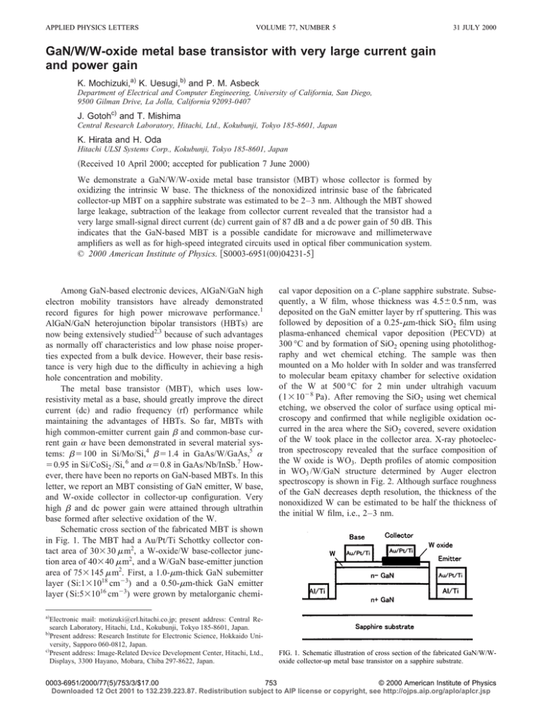
APPLIED PHYSICS LETTERS VOLUME 77, NUMBER 5 31 JULY 2000 GaNÕWÕW-oxide metal base transistor with very large current gain and power gain K. Mochizuki,a) K. Uesugi,b) and P. M. Asbeck Department of Electrical and Computer Engineering, University of California, San Diego, 9500 Gilman Drive, La Jolla, California 92093-0407 J. Gotohc) and T. Mishima Central Research Laboratory, Hitachi, Ltd., Kokubunji, Tokyo 185-8601, Japan K. Hirata and H. Oda Hitachi ULSI Systems Corp., Kokubunji, Tokyo 185-8601, Japan 共Received 10 April 2000; accepted for publication 7 June 2000兲 We demonstrate a GaN/W/W-oxide metal base transistor 共MBT兲 whose collector is formed by oxidizing the intrinsic W base. The thickness of the nonoxidized intrinsic base of the fabricated collector-up MBT on a sapphire substrate was estimated to be 2–3 nm. Although the MBT showed large leakage, subtraction of the leakage from collector current revealed that the transistor had a very large small-signal direct current 共dc兲 current gain of 87 dB and a dc power gain of 50 dB. This indicates that the GaN-based MBT is a possible candidate for microwave and millimeterwave amplifiers as well as for high-speed integrated circuits used in optical fiber communication system. © 2000 American Institute of Physics. 关S0003-6951共00兲04231-5兴 Among GaN-based electronic devices, AlGaN/GaN high electron mobility transistors have already demonstrated record figures for high power microwave performance.1 AlGaN/GaN heterojunction bipolar transistors 共HBTs兲 are now being extensively studied2,3 because of such advantages as normally off characteristics and low phase noise properties expected from a bulk device. However, their base resistance is very high due to the difficulty in achieving a high hole concentration and mobility. The metal base transistor 共MBT兲, which uses lowresistivity metal as a base, should greatly improve the direct current 共dc兲 and radio frequency 共rf兲 performance while maintaining the advantages of HBTs. So far, MBTs with high common-emitter current gain  and common-base current gain ␣ have been demonstrated in several material systems:  ⫽100 in Si/Mo/Si,4  ⫽1.4 in GaAs/W/GaAs,5 ␣ ⫽0.95 in Si/CoSi2 /Si, 6 and ␣ ⫽0.8 in GaAs/Nb/InSb.7 However, there have been no reports on GaN-based MBTs. In this letter, we report an MBT consisting of GaN emitter, W base, and W-oxide collector in collector-up configuration. Very high  and dc power gain were attained through ultrathin base formed after selective oxidation of the W. Schematic cross section of the fabricated MBT is shown in Fig. 1. The MBT had a Au/Pt/Ti Schottky collector contact area of 30⫻30 m2, a W-oxide/W base-collector junction area of 40⫻40 m2, and a W/GaN base-emitter junction area of 75⫻145 m2. First, a 1.0-m-thick GaN subemitter layer (Si:1⫻1018 cm⫺3) and a 0.50-m-thick GaN emitter layer (Si:5⫻1016 cm⫺3) were grown by metalorganic chemi- cal vapor deposition on a C-plane sapphire substrate. Subsequently, a W film, whose thickness was 4.5⫾0.5 nm, was deposited on the GaN emitter layer by rf sputtering. This was followed by deposition of a 0.25-m-thick SiO2 film using plasma-enhanced chemical vapor deposition 共PECVD兲 at 300 °C and by formation of SiO2 opening using photolithography and wet chemical etching. The sample was then mounted on a Mo holder with In solder and was transferred to molecular beam epitaxy chamber for selective oxidation of the W at 500 °C for 2 min under ultrahigh vacuum (1⫻10⫺8 Pa). After removing the SiO2 using wet chemical etching, we observed the color of surface using optical microscopy and confirmed that while negligible oxidation occurred in the area where the SiO2 covered, severe oxidation of the W took place in the collector area. X-ray photoelectron spectroscopy revealed that the surface composition of the W oxide is WO3. Depth profiles of atomic composition in WO3 /W/GaN structure determined by Auger electron spectroscopy is shown in Fig. 2. Although surface roughness of the GaN decreases depth resolution, the thickness of the nonoxidized W can be estimated to be half the thickness of the initial W film, i.e., 2–3 nm. a兲 Electronic mail: motizuki@crl.hitachi.co.jp; present address: Central Research Laboratory, Hitachi, Ltd., Kokubunji, Tokyo 185-8601, Japan. b兲 Present address: Research Institute for Electronic Science, Hokkaido University, Sapporo 060-0812, Japan. c兲 Present address: Image-Related Device Development Center, Hitachi, Ltd., Displays, 3300 Hayano, Mobara, Chiba 297-8622, Japan. FIG. 1. Schematic illustration of cross section of the fabricated GaN/W/Woxide collector-up metal base transistor on a sapphire substrate. 0003-6951/2000/77(5)/753/3/$17.00 753 © 2000 American Institute of Physics Downloaded 12 Oct 2001 to 132.239.223.87. Redistribution subject to AIP license or copyright, see http://ojps.aip.org/aplo/aplcr.jsp 754 Appl. Phys. Lett., Vol. 77, No. 5, 31 July 2000 Mochizuki et al. FIG. 2. Depth profiles of atomic composition in W-oxide/W/GaN structure determined by Auger electron spectroscopy. Next, a 1.5-m-thick SiO2 film was deposited on the selectively oxidized W film by PECVD at 300 °C. This was followed by base mesa photolithography, wet chemical etching of the SiO2, and reactive ion etching 共RIE兲 of the W using CF4. After removing the photoresist with acetone, 0.50-m-thick GaN emitter and 0.15-m-thick GaN subemitter were etched by CCl2F2 RIE using the SiO2 as a mask. The SiO2 mask was then removed by wet chemical etching, and an Al/Ti emitter electrode was formed on the GaN subemitter surface by a lift-off technique followed by alloying at 650 °C for 40 s. Finally, a Au/Pt/Ti electrode was formed by a liftoff technique on the W-oxide as a Schottky collector contact, and on the W base and the Al/Ti emitter electrodes as probing pads. Transmission line model measurement showed that the sheet resistance of the extrinsic base 共nonoxidized W兲 was 0.40 k⍀/sq, while that of the intrinsic base 共partially oxidized W兲 was 7.0 k⍀/sq. This indicates that the mobility in W is severely degraded when the film thickness becomes less than 5 nm. Figure 3共a兲 shows the common-emitter current–voltage characteristics measured at room temperature using an HP 4155 curvetracer. The large collector leakage with a turn-on voltage of 0.4 V indicates that the Au/Pt/Ti collector electrode touched the n-GaN emitter through pores in the W base.5 Careful control of the W deposition condition is expected to decrease the collector leakage. The slope of 53 ⍀ in Fig. 3共a兲 corresponds to the sum of emitter and collector resistance. Here we define ⌬I C as the difference between the collector current I C at a certain base current I B and the I C at I B ⫽0. Figure 3共b兲 shows the collector-to-emitter voltage (V CE) dependence of the ⌬I C with I B from 20 to 80 nA 共20 nA step兲. When I B ⭌100 nA, ⌬I C did not increase from the results with I B ⫽80 nA. We have not yet understood what caused the ⌬I C saturation. The peak  reached 2.2 ⫻104 (87 dB) at V CE⫽4.7 V when I B ⫽20– 40 nA. This  almost agrees with the observed ␣ ⫽0.999 95 in commonbase current–voltage characteristics. The dc power gain was calculated from the curves of I B ⫽20 and 40 nA in Fig. 3共b兲 with the obtained base-emitter voltage, and the result is shown in Fig. 4 as a function of the mean ⌬I C between ⌬I C (I B ⫽20 nA) and ⌬I C (I B ⫽40 nA). The maximum dc power gain of 50 dB was achieved at ⌬I C ⫽0.90 mA. The FIG. 3. 共a兲 Common-emitter current–voltage characteristics with base currents of 80 nA 共open circles兲 and 0 共solid triangles兲. 共b兲 Collector-to-emitter voltage dependence of ⌬I C , which is the difference between the collector current I C at a base current I B of 20–80 nA 共20 nA step兲 and the I C at I B ⫽0. FIG. 4. Small-signal power gain as a function of the mean ⌬I C between ⌬I C (I B ⫽20 nA) and ⌬I C (I B ⫽40 nA). Downloaded 12 Oct 2001 to 132.239.223.87. Redistribution subject to AIP license or copyright, see http://ojps.aip.org/aplo/aplcr.jsp Mochizuki et al. Appl. Phys. Lett., Vol. 77, No. 5, 31 July 2000 detailed mechanisms of current flow leading to the very high  are not yet fully understood; however, the large incremental power gain unequivocally confirms transistor operation. No alternating current measurements of the device characteristics have been made. It is likely that the device has the potential for very high cutoff frequency ( f T ), as a result of the ultrashort dimensions involved. Although the maximum oscillation frequency ( f max) may be limited due to large base-collector capacitance in the present implementation, very high f max can be expected by increasing the thickness of the W oxide, particularly because of the potentially low resistance of the metal base. In conclusion, the fabricated collector-up GaN/W/Woxide metal base transistor on a sapphire substrate showed a very large small-signal dc current gain of 87 dB and a dc power gain of 50 dB. These results indicate that the GaNbased MBT is a possible candidate for microwave and millimeterwave amplifiers as well as for high-speed integrated circuits used in optical fiber communication system. 755 The authors would like to thank D. Qiao of Department of Electrical and Computer Engineering, University of California, San Diego, for his support for making ohmic contacts to GaN. The author K. M. is grateful to Dr. I. Ohbu of Central Research Laboratory, Hitachi, Ltd., Japan for his support for preparing the W-deposited GaN on sapphire wafers. 1 S. T. Sheppard, K. Doverspike, W. L. Pribble, S. T. Allen, J. W. Palmour, L. T. Kehias, and T. J. Jenkins, 56th Annual Device Research Conference Digest, Charlotsville, VA, 1998. 2 L. S. McCarthy, P. Kozodoy, M. J. W. Rodwell, S. P. Denbaars, and U. K. Mishra, IEEE Electron Device Lett. 20, 277 共1999兲. 3 J. B. Limb, L. McCarthy, L. P. Kozodoy, H. Xing, J. Ibbetson, Y. Smorchkova, S. P. Denbaars, and U. K. Mishra, Electron. Lett. 35, 1671 共1999兲. 4 J. Lindmayer, Proc. IEEE 52, 1751 共1964兲. 5 G. E. Derkits, Jr., J. P. Harbison, J. Levkoff, and D. M. Hwang, Appl. Phys. Lett. 48, 1220 共1986兲. 6 R. T. Tung, A. F. Levi, and J. M. Gibson, Appl. Phys. Lett. 48, 635 共1986兲. 7 T. Kobayashi, H. Sakai, and M. Tonouchi, Electron. Lett. 22, 659 共1986兲. Downloaded 12 Oct 2001 to 132.239.223.87. Redistribution subject to AIP license or copyright, see http://ojps.aip.org/aplo/aplcr.jsp
![Structural and electronic properties of GaN [001] nanowires by using](http://s3.studylib.net/store/data/007592263_2-097e6f635887ae5b303613d8f900ab21-300x300.png)
