Homework #1 Solutions - Stanford Microsystems Group
advertisement
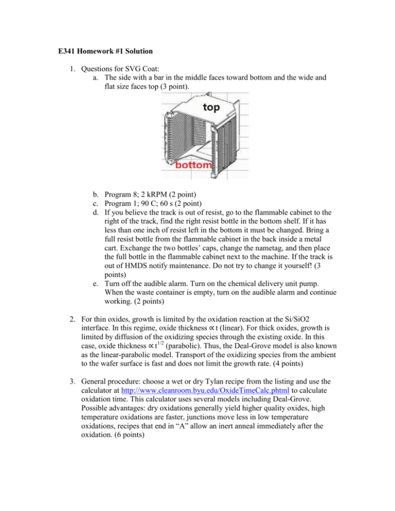
E341 Homework #1 Solution 1. Questions for SVG Coat: a. The side with a bar in the middle faces toward bottom and the wide and flat size faces top (3 point). b. Program 8; 2 kRPM (2 point) c. Program 1; 90 C; 60 s (2 point) d. If you believe the track is out of resist, go to the flammable cabinet to the right of the track, find the right resist bottle in the bottom shelf. If it has less than one inch of resist left in the bottom it must be changed. Bring a full resist bottle from the flammable cabinet in the back inside a metal cart. Exchange the two bottles’ caps, change the nametag, and then place the full bottle in the flammable cabinet next to the machine. If the track is out of HMDS notify maintenance. Do not try to change it yourself! (3 points) e. Turn off the audible alarm. Turn on the chemical delivery unit pump. When the waste container is empty, turn on the audible alarm and continue working. (2 points) 2. For thin oxides, growth is limited by the oxidation reaction at the Si/SiO2 interface. In this regime, oxide thickness ∝ t (linear). For thick oxides, growth is limited by diffusion of the oxidizing species through the existing oxide. In this case, oxide thickness ∝ t1/2 (parabolic). Thus, the Deal-Grove model is also known as the linear-parabolic model. Transport of the oxidizing species from the ambient to the wafer surface is fast and does not limit the growth rate. (4 points) 3. General procedure: choose a wet or dry Tylan recipe from the listing and use the calculator at http://www.cleanroom.byu.edu/OxideTimeCalc.phtml to calculate oxidation time. This calculator uses several models including Deal-Grove. Possible advantages: dry oxidations generally yield higher quality oxides, high temperature oxidations are faster, junctions move less in low temperature oxidations, recipes that end in “A” allow an inert anneal immediately after the oxidation. (6 points) 4. (3 points) 5. The three methods are: (6 points) a. Ion implantation: POCl3 and BBr3 at tylan5 and tylan6 b. In situ doping of epitaxial silicon: epi2 c. In situ doping of LPCVD polysilicon: thermcopoly1, thermcopoly2 6. Since this is the handle layer, and I do not care too much about the sidewalls, I would chose FASTDEEP. The website lists FASTDEEP as having an etch rate of up to 5 um/min. The required etch time is 350 um divided by 5 um/min, yielding 70 minutes. The actual etch rate depends on exposed silicon area, which is why it is important to run a test wafer first. (3 points) 7. Methods: (6 points) a. Use an anisotropic etch like TMAH or KOH on a single crystal silicon. b. For an SOI, use an isotropic etch like Dry: XeF2 in Xactix; SF6 in drytek2, lampoly, stsetch or Wet: HNA (hydrofluoric, nitric, acetic) at wbgeneral, which will etch down to the BOX layer with round sidewalls. The etch stops at the BOX layer, thus giving the appearance of a flat bottom. For a single crystal silicon, first etch with DRIE for a bit to get a rectangular well. Then again use the aforementioned isotropic etchants to get the same round sidewalls and flat trench bottom. Total: 40 points

