Supplemental material
advertisement
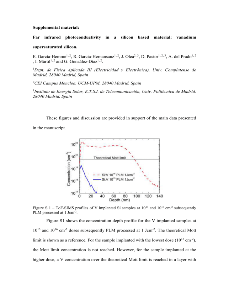
Supplemental material: Far infrared photoconductivity in a silicon based material: vanadium supersaturated silicon. E. García-Hemme1, 2, R. Garcia-Hernansanz1, 2, J. Olea2, 3, D. Pastor1, 2, 3, A. del Prado1, 2 , I. Mártil1, 2 and G. González-Díaz1, 2. 1 Dept. de Física Aplicada III (Electricidad y Electrónica), Univ. Complutense de Madrid, 28040 Madrid, Spain 2 CEI Campus Moncloa, UCM-UPM, 28040 Madrid, Spain 3 Instituto de Energía Solar, E.T.S.I. de Telecomunicación, Univ. Politécnica de Madrid. 28040 Madrid, Spain These figures and discussion are provided in support of the main data presented in the manuscript. Figure S 1 – ToF-SIMS profiles of V implanted Si samples at 1013 and 1016 cm-2 subsequently PLM processed at 1 Jcm-2. Figure S1 shows the concentration depth profile for the V implanted samples at 1013 and 1016 cm-2 doses subsequently PLM processed at 1 Jcm-2. The theoretical Mott limit is shown as a reference. For the sample implanted with the lowest dose (1013 cm-2), the Mott limit concentration is not reached. However, for the sample implanted at the higher dose, a V concentration over the theoretical Mott limit is reached in a layer with an approximate thickness of 100 nm. Theoretically, the delocalization transition point could have been surpassed for this sample. Figure S 2 - High resolution TEM images of V implanted Si sample at 1013 cm-2 dose and subsequently PLM processed at 1 Jcm-2. Figure S2 shows the high degree of crystallization obtained in the V implanted Si sample at 1013 cm-2 and PLM processed at 1 Jcm-2. Figure S 3 - Sheet conductance as a function of the temperature for the Si implanted Si at 10 16 cm-2, the V implanted Si at 1013 cm-2 and the V implanted at 1016 cm-2. All these samples were subsequently PLM processed at 1 Jcm-2. Also a reference silicon substrate is shown. Dashed lines represent the values obtained from the substraction of the V implanted Si at 10 16 cm-2 and the Si reference substrate. Figure S3 shows the sheet conductance as a function of the temperature for the V implanted samples at 1013 and 1016 cm-2 doses and PLM at 1 Jcm-2 and the Si implanted Si sample at 1016 cm-2 dose and PLM at 1 Jcm-2. Also, a reference silicon unimplanted substrate is presented. We can observe the expected behavior for the Si unimplanted substrate, i.e. an increase of the sheet conductance as the temperature decreases due to the reduction of the phonon scattering and an abrupt decrease of the sheet conductance at very low temperatures due to the carrier concentration freeze-out effect. The Si implanted Si sample and the V implanted sample at the lowest dose 1013 cm-2 show a sheet conductance behavior almost equal to the Si substrate. These results suggest that, by one side, the defective layer of the Si implanted Si sample does not significantly affect the transport properties of the whole sample. By the other side, the implantation of V with a 1013 cm-2 does not affect the transport properties despite the high V concentration. However, the V implanted sample at the highest dose (1016 cm-2) shows a different trend. This sample increases its sheet conductance as the temperature decreases, but at a given temperature of 113 K the sheet conductance decrease as the temperature decreases, approaching to an almost constant value at very low temperatures of 0.55 𝑚𝑆 without showing a concentration freeze out effect. We have to take into account that this sample presents a V concentration over the theoretical insulator-metal transition and then a band of allowable states could be formed from the delocalization of the V deep levels states in the implanted and PLM layer, i.e. an intermediate band (IB). Therefore the absence of the freeze out effect would be coherent with the proposed Mott transitions since a semi-filled IB could result in a metallic behavior. Therefore we can assume for this sample a parallel bilayer structure formed by an IB material in the implanted layer and a silicon substrate. The total sheet conductance of the two layer associated in parallel is given by 𝐺𝑇 = 𝐺𝐼𝐵 + 𝐺𝑆𝑖 , where 𝐺𝐼𝐵 is the sheet conductance of the IB material and 𝐺𝑆𝑖 is the sheet conductance of the Si substrate. For temperatures lower than 113K, this sample is going through an electrical decoupling between the IB material layer and the Si substrate, otherwise 𝐺𝑇 could not be lower than the sheet conductance of any of the conduction branches (Si substrate or IB material layer). Therefore, for the lower temperature range we are measuring only the electrical transport properties of the IB material (𝐺𝐼𝐵 ). In the temperature range where the bilayer is coupled (113 K – 300 K), the dashed line represents the values obtained from the subtraction of the total sheet conductance and the Si reference substrate sheet conductance, i.e. 𝐺𝐼𝐵 = 𝐺𝑇 − 𝐺𝑆𝑖 . This magnitude represents the IB material sheet conductance when the two layers are coupled. We can observe that it shows a very low temperature dependence and that its value tends to the one measured at low temperatures. This electrical decoupling effect and metallic behavior has been also observed in the Ti supersaturated Si1 and Co supersaturated Si.2 This electrical behavior has been satisfactorily explained and reproduced by means of an analytical model which takes into account the parallel bilayer structure formed by the IB material and the Si substrate.3 Moreover, this electrical decoupling effect cannot be associated with the implantation/PLM induced effects since the Si implanted Si sample shows the same transport properties than the Si unimplanted reference substrate. 1. J. Olea, D. Pastor, E. Garcia-Hemme, R. Garcia-Hernansanz, A. del Prado, I. Martil and G. Gonzalez-Diaz, Thin Solid Films 520, 6614-6618 (2012). 2. Y. Zhou, F. Liu and X. Song, Journal of Applied Physics 113, 103702 (2013). 3. J. Olea, G. Gonzalez-Diaz, D. Pastor, I. Martil, A. Marti, E. Antolin and A. Luque, Journal of Applied Physics 109, 8 (2011).

