qna
advertisement
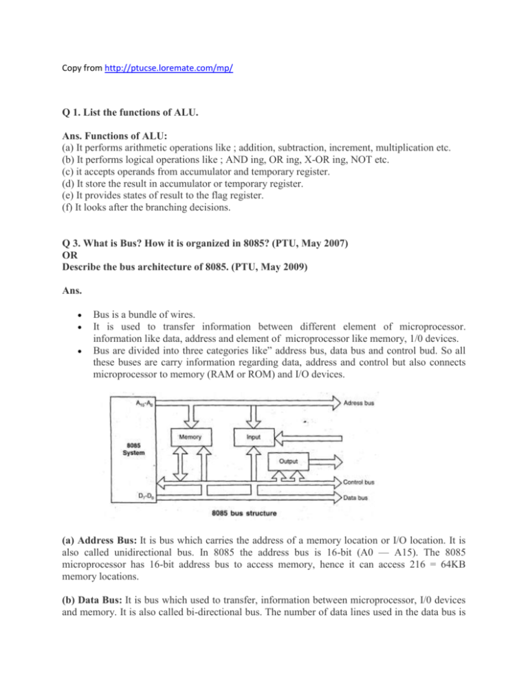
Copy from http://ptucse.loremate.com/mp/ Q 1. List the functions of ALU. Ans. Functions of ALU: (a) It performs arithmetic operations like ; addition, subtraction, increment, multiplication etc. (b) It performs logical operations like ; AND ing, OR ing, X-OR ing, NOT etc. (c) it accepts operands from accumulator and temporary register. (d) It store the result in accumulator or temporary register. (e) It provides states of result to the flag register. (f) It looks after the branching decisions. Q 3. What is Bus? How it is organized in 8085? (PTU, May 2007) OR Describe the bus architecture of 8085. (PTU, May 2009) Ans. Bus is a bundle of wires. It is used to transfer information between different element of microprocessor. information like data, address and element of microprocessor like memory, 1/0 devices. Bus are divided into three categories like” address bus, data bus and control bud. So all these buses are carry information regarding data, address and control but also connects microprocessor to memory (RAM or ROM) and I/O devices. (a) Address Bus: It is bus which carries the address of a memory location or I/O location. It is also called unidirectional bus. In 8085 the address bus is 16-bit (A0 — A15). The 8085 microprocessor has 16-bit address bus to access memory, hence it can access 216 = 64KB memory locations. (b) Data Bus: It is bus which used to transfer, information between microprocessor, I/0 devices and memory. It is also called bi-directional bus. The number of data lines used in the data bus is equal to the size of data word being written or read. Data bus is time multiplexed with lower order address bus. (c) Control Bus: It is bus which is necessary to Control the direction of data flow on the bidirectional data bus and to differentiate between a memory address and an I/O address. Some of the control bus signals are follows: (I) Memory read (ii) Memory writer (iii) I/O read (iv) I/O writes. Q 4. What is a parity flag? When is it affected? (PTU, May 2004) Ans. The parity flag (P) is one among the five status flags that the Intel 8085 microprocessor contains. The .parity status flag P is set to 1, if the result of an arithmetic or logical operation contains even number of is. It is reset i.e. it is 0, if the result contains odd number of is. For e.g. The data byte 00000011 has even parity even if the magnitude of the number is odd. Q 5. Write two different methods to clear the Accumulator. (PTU, Dec. 2005, 2004) Ans. • MVI A, 00H • XRA A ; Direct Addressing ; Accumulator XOR A 01000011 01000011 00009000 So accumulator will be cleaned Q 6 Why demultiplexing of AD7, AD0 is required’ (PTU, Dec 2004, May 2004) Ans Basically, ALE signal give us the information that which of the bus data bus or address bus we are using ALE signal is used to demultiplexing the bus The bus AD7 — AD0 is connected as the input to latch 74LS373 ALE signal is attached to enable pin of the latch (4) CC — output control ALE when high — latch is transparent output changes according to input data To reduce the number of pins to make it compact one and easy to use data bus and address bus is demultiplexed Data bus — 8 bits Address bus —* 16 bits So 8 bits of address bus and data bus are multiplex and the ALE (Address I enable) is used to demultiplexed them Q7 What is a PSW (PTU, Dec 2005, 2008 Ans. PSW: Program status word which implies to check the status of flags. S — sign flag — if bit D is set, sign flag is set. This flag is used with signed numbers. If D7 is set then number is viewed as negative number. Z — zero flag — zero flag is set if the ALU operation results in zero and the flag is reset when result is not zero. AC — Auxilliary carry flag — when carry is generated by the digit 03 and passed on to digit D4, the AC flag is set. Flag is used only internally for BCD. P — Parity flag — If accumulator has an even number of is, flag is set. If it has an odd number of is, the flag is reset. CY — Carry flag — If an arithmetic operations results in carry, the carry flag is set. Q 10 Explain the requirement of a program counter in 8085 microprocessor Ans Program counter gives us the information about the next instruction to be executed PC has the address or point out the address of the next Instruction to be executed In call and ret statements the word and registers are temporary registers used to store the temporary address Then program counter will jump to the call or ret instruction address Q 19. What happens in a single board microcomputer when the power is turned on any reset key is pushed? (PTU, Dec. 2008) Ans. After resetting the single board microcomputer starts executing instructions from 000H onwards Q 24. What is the various status signals used in 8085? (PTU, May 2009) Ans. 1. Address latch enable (ALE) 2. Input outputs/memory (IO/M) 3. Status signals (S1 and S0) 4. Read (RD) 5. Write (W) 6. READY. Q29. Explain the function of ALE and 10/ M signals of the 8085 microprocessor. (PTU, May 2007) Ans. 1. ALE (Address Latch Enable): It is a output signal of 8085 microprocessor. It is basically used to give information of AD0 — AD7 contents. It is a positive going pulse generated during the first clock cycle of a machine cycle. If pulse is high it indicates that the contents of AD0 — AD7 are address. On the other hand if it is low it indicates that the contents are data ALE=1 = Address ALE=0=Data The ALE signal is used to separate AD0 — AD7 (i.e. demultiplex) to A0 — A7 and D0 — D7. 2. Input Output/Memory (I0/Ti): It is an output status signal of 8085 microprocessor. It is basically used to give information of operation to be performed with memory or I/O device. If the lO/ii pin is low (i.e. lO/TI = 0), the microprocessor is performing a memory related operation. On the other hand, if the lO/T pin is high (i.e. IO/M = 1), the microprocessor is performing an I/O device related operation. IO/M = 0 Memory related operation. lO/M = 1 = I/O device related operation. Q 32. Draw a schematic to demultiplex bus AD7 — AD0 using any octal latch. (PTU, Dec. 2007) Ans. The 8085 microprocessor is used IC 74LS373 to latch the address of 8085. Basically latch is consists of 8 flip flops. Generally we used D-flip flops (Delay). The clock of these flip flops are connected together and available as a output pin called enable. Working : The address will appear on AD0 AD7 lines. The ALE will go high and forcing Enable = 1. This will make latch enable and ready to work. Before address disappears ALE = 0. This will make latch disable. AD0 — AD7 will now be used as data bus. Hence, AD0 — AD7 (low order) address bus of the 8085 microprocessor is multiplexed (timeshared) with the data bus. The buses need to be demultiplexed. Q 34 What are the functions of stack pointer and program Ans. Functions of the stack pointer: (i) It is used ‘for holding the address of program memory counter? (ii) It isaiways points to the next instruction to be fetched. (iii) The size of program counter depends upon the number of address bits. (iv) In Jump and call instructions, the address followed by the jump and call instructions is placed in the program counter. Functions of stack pointer: (i) It is used to keep the track of data stored on stack. (ii) Stack pointer is a reserved• portion of memory where information can be stored. This memory area is referred to as a stack area. (iii) Stack pointer is a 16-bit register used for defining the stack starting address. It is always points at the top of the stack. (iv) Stack pointer is decremented after each stack write operation and it is incremented after each stack read operation. (v) The stack pointer is loaded with an initial value by the means of a transfer type instruction. Initial value must be the highest address of an assigned stack in the memory. Q 35. What are the various registers used in 8085? (PTU, Dec. 2009) OR What do you meant by register? Discuss various registers of 8085 iR (PTU, May 2008) OR Write the internal data operations and 8085 programmable registers. (PTU, May 2007) Ans. Registers: It is used to store data or address. It is a set of flip flops which are used for temporary storage of information (data or address or instruction). It consists of PIPO (Parallel in Parallel Out) Registers. The 8085 microprocessor consists of following registers 1. Temporary data register 2. Temporary registers W and Z 3. 8-bit accumulator 4. Flag register 5. Six general purpose registers (B, C, D, E, H and L) 6. 16-bit program counter : 7. 16-bit stack pointer 8. Instruction register. 1. Temporary Data Register : This register is also called as operand register. It provides operands to the ALU. It is a 8-bit register and not available to user. 2. Temporary Registers (W and Z) : These registers are used by control section to hold the data during an arithmetic or logical operation. It is hold 8 bit data. These register are not available to user. They are internally used by the microprocessor. e.g.: (a) XCHG (exchange) (b) XTHL (exchange top of stack with registers H and L). 3. 8-bit accumulator : This register is used to store the first input as well as result of any calculation is also stored in accumulator. The accumulator is identified as register A. It is an 8-bit general purpose register. 4. Flag register : The flag register is give the status of the result. It is a part of arithmetic and logical section. It indicates some condition produced by the execution of an instruction. The 8085 microprocessor consists of five flags. (a) Sign Flag (S) (b) Zero Flag (Z) (c) Auxiliary Carry Flag (AC) (d) Parity Flag (P) (e) Carry Flag (CV) 5. Six general purpose registers (B, C, D, E, H and L) : The 8085 microprocessor contains 6 general purpose registers of 8 bits each, named as B, C, D, E, H and L. These registers are programmable by user. They are used to hold data, results of arithmetic and logical operations and address of data memory. The valid register pairs available are BC, DE and HL. The user cannot form a register pair of his/her choice. 6. 16-bit program counter (PC) : The program counter is used to hold the address of program memory. It always points to the next instruction to be fetched i.e. it holds the memory address of the next instruction to be executed. 7. 16-bit Stack Pointer (SP): Stack is a reserved portion of memory where information can be stored to taken back under software control. This memory area is referred to as stack area. The stack pointer is auto decremented by 2 after PUSH operation and auto incremented by 2 after POP operation. 8. Instruction Register: An instruction fetched from memory is temporarily stored in Instruction Register before decoding. So after fetching instruction from memory, microprocessor stores it in the instruction register and after this it is decoded. 1. Register Section : It consists of PIPO (Parallel in parallel out)’register. Register contains a set of. binary storage cells/flip flops with facilities of read and write. It. is used for temporary storage of instructions also used for data and address. Hence, the number of bits in a register is equal to data or address depending on the application. Fig. shows register section of 8085. Architecture of 8085 consists of following registers (a) Temporary data register (b) Instruction registers (c) 16-bit stack pointer (d) Flag register (e) Temporary registers W and Z (f) 8-bit accumulator (g) Six general purpose registers (B, C, D, E, H and L) (h) 16-bit program counter. Accumulator: It is 8-bit general purpose register of 8085. It has some special functions due to this it is also known as special register. Following are special functions of accumulator: (a) It has to private one of operand for any ALU operations. (b) It is used for accumulation. (c) Whenever a data is read from input device it comes in accumulator and similarly output device gets data from the accumulator. Status or Flag Register : Flag is a flip-flop. It indicates some condition produced by execution of an instruction. (a) The flag register 8085 consists of five flags. It is connected to the ALU. (b) When any operation is performed by ALU result is transferred on internal data bus and status of result will be stored in flip-flops. Instruction Register: 1. The register is not accessible to user. 2. Instruction register holds the opcode of instruction that is decoded and executed. 3. This opcode is sent for instruction decoder to select one of 256 alternatives. Program Counter: 1. Used for holding the address of program memory. 2. In reset condition, the program counter is set to 000H, means that the address of first instruction to be fetched and executed. 3. The size of program counter depends upon the number of address bits. 4. In case of JUMP and call instructions, the address followed by JUMP and call instructions is placed in program counter. If the condition is satisfied then 8085 fetches the next instruction from the new adçiress specified by JUMP or call instructions. 5. During instruction fetch operation, the contents of program counter on the address bus and it fetches first byte of instruction from memory location. Stack Pointer: 1. It is portion of memory where information can be stored or taken back. This memory area is known as stack area. 2. It is 16-bit register used for defining the stack starting address. 3. Used to keep track of data store don stack. 4. It is loaded with an initial value by means of transfer type instruction. Arithmetic Logic Unit (ALU) : This section processes all data i.e. it perform arithmetic and logic operations. 1. It performs addition, subtraction and logical, operations like AND, OR, EX-OR. 2. ALU is always controlled by timing and control circuits. 3. It looks after the branching decisions. 4. It provides status of result to the flag register. Q7. Explain what is SIM. Ans. This is Set Interrupt Mask • This is a 1 byte instructions. • This instructions reads the contents of the accumulator and enables or disables the -interrupts according to the contents of the accumulator. • Bits W7 and W6 of accumulator are used for serial I/O and do not affect the interrupts. D6 1 enables the serial I/O Q 13 Why the number of 0/P ports in peripheral mapped I/O is restricted to 256’ (PTU, May 2008) Ans In I/O addressing mode 8085 has capability of 8 bit I/O address through which it can address 255 I/O ports Q 1. List categories of 8085 instructions that manipulate data. Ans. 8085 instruction, are: 1. Data transfer instructions : (a) MOV (b) MVI (c) LDA (d) STA 2. Arithematic Instructions (a) ADD (b) AD) (c)SUB (ci) SBI (f) DCR 3. Logical Instructions (a) ANA (b) ORI (c)CMP (d) RLC (e) RRC 4. Branch Instructions (a) JMP (b) CALL 5. Stack and machine control instructions (a) PUSH (b) POP. Q 5. What is difference between CALL, RET and PUSH, POP’ instructions?. Ans. Q 10. What happens when RET instruction is executed? Ans When RET instruction is executed program control is transferred from the subroutine to the calling program. The return address is taken from stack, this address is loaded in PC and the program execution begins at address taken from stack. Thus, program control is transferred to the next instruction after call En the main program.
