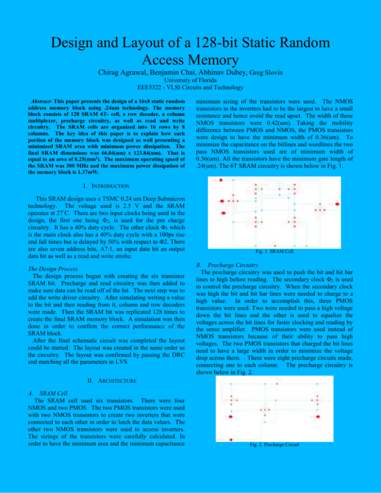
Design and Layout of a 128-bit Static Random
Access Memory
Chirag Agrawal, Benjamin Chai, Abhinav Dubey, Greg Slovin
University of Florida
EEE5322 - VLSI Circuits and Technology
Abstract- This paper presents the design of a 16x8 static random
address memory block using .24um technology. The memory
block consists of 128 SRAM 6T- cell, a row decoder, a column
multiplexer, precharge circuitry, as well as read and write
circuitry. The SRAM cells are organized into 16 rows by 8
columns. The key idea of this paper is to explain how each
portion of the memory block was designed as well presenting a
minimized SRAM area with minimum power dissipation. The
final SRAM dimensions was 66.84(um) x 123.84(um). That is
equal to an area of 8.25(mm2). The maximum operating speed of
the SRAM was 300 MHz and the maximum power dissipation of
the memory block is 1.37mW.
minimum sizing of the transistors were used. The NMOS
transistors in the inverters had to be the largest to have a small
resistance and hence avoid the read upset. The width of these
NMOS transistors were 0.42(um). Taking the mobility
difference between PMOS and NMOS, the PMOS transistors
were design to have the minimum width of 0.36(um). To
minimize the capacitance on the bitlines and wordlines the two
pass NMOS transistors used are of minimum width of
0.36(um). All the transistors have the minimum gate length of
.24(um). The 6T SRAM circuitry is shown below in Fig. 1.
I. INTRODUCTION
This SRAM design uses a TSMC 0.24 um Deep Submicron
technology. The voltage used is 2.5 V and the SRAM
operates at 27°C. There are two input clocks being used in the
design, the first one being Φ2, is used for the pre charge
circuitry. It has a 40% duty cycle. The other clock Φ1 which
is the main clock also has a 40% duty cycle with a 100ps rise
and fall times but is delayed by 50% with respect to Φ2. There
are also seven address bits, A7:1, an input data bit an output
data bit as well as a read and write strobe.
The Design Process
The design process began with creating the six transistor
SRAM bit. Precharge and read circuitry was then added to
make sure data can be read off of the bit. The next step was to
add the write driver circuitry. After simulating writing a value
to the bit and then reading from it, column and row decoders
were made. Then the SRAM bit was replicated 128 times to
create the final SRAM memory block. A simulation was then
done in order to confirm the correct performance of the
SRAM block.
After the final schematic circuit was completed the layout
could be started. The layout was created in the same order as
the circuitry. The layout was confirmed by passing the DRC
and matching all the parameters in LVS.
Fig. 1. SRAM Cell
B. Precharge Circuitry
The precharge circuitry was used to push the bit and bit bar
lines to high before reading. The secondary clock Φ2 is used
to control the precharge circuitry. When the secondary clock
was high the bit and bit bar lines were needed to charge to a
high value. In order to accomplish this, three PMOS
transistors were used. Two were needed to pass a high voltage
down the bit lines and the other is used to equalize the
voltages across the bit lines for faster clocking and reading by
the sense amplifier. PMOS transistors were used instead of
NMOS transistors because of their ability to pass high
voltages. The two PMOS transistors that charged the bit lines
need to have a large width in order to minimize the voltage
drop across them. There were eight precharge circuits made,
connecting one to each column. The precharge circuitry is
shown below in Fig. 2.
II. ARCHITECTURE
A.
SRAM Cell
The SRAM cell used six transistors. There were four
NMOS and two PMOS. The two PMOS transistors were used
with two NMOS transistors to create two inverters that were
connected to each other in order to latch the data values. The
other two NMOS transistors were used to access inverters.
The sizings of the transistors were carefully calculated. In
order to have the minimum area and the minimum capacitance
Fig. 2. Precharge Circuit
C. Sense Circuitry
The sense circuitry was created in order to read the value
stored in the SRAM cell. As clocked sense amplifier saves the
power it was used to determine the difference in voltage
between the bit and bit bar lines when the SRAM cell was
accessed to read. It is implemented using the two PMOS
isolation transistor and a regenerative feedback circuitry.
When the sense enable is high and is in phase with clock, two
isolation NMOS transistors are turned on to connect the bit
and bit bar lines to the sense amplifier. An isolation PMOS
and NMOS transistor of sense circuitry were also turned on at
the same time connecting VDD and ground to the amplifier
using inverter. These isolation transistors are used to save the
power by keeping the sense amplifier off when it is not in use.
All NMOS and PMOS transistors used the minimum width of
.36(um) in order to conserve space in the layout. The sensing
circuitry is shown below in Fig. 3.
implement as multiplexer switch. The input reording has been
done to minimize the propagation delay considering the
probability of the inputs. The column decoder circuitry is
shown below in Fig. 5.
Fig. 5. Column Decoder
Fig. 3. Sense Circuitry
D. Write Driver
The write driver circuitry consists of four NMOS transistors
and an inverter. When the write strobe is high, the top two
NMOS transistors are on and hence the bit and bit bar lines are
connected to data line transistors .As a result either of them is
pulled down depending on the data line bit. All of the
transistors in the write driver circuitry have the minimum
width of 0.36(um) in order to conserve space in the layout.
The write driver circuitry is shown below in Fig. 4.
F. Row Decoder
The row decoder is a 4:16 static decoder implemented using
the predecoder stage. Because of predecoder stage it helps to
minimize the transistor count and also reduces the propagation
delay by a factor of 4. Using address lines A1:4, the decoder
circuitry chooses which word line to turn on. Each output of
the decoder is anded with the primary clock, Φ1. This avoids
any word lines from being high when the clock is low. As a
result of which no two rows are activated at the same time.
Two input NOR gates are used instead of larger input NOR
gates in the predecoder stage to limit the fan in capacitances
and the two inputs nand gates are used in the output stage with
the inverters acting as buffers to drive the large loads. Since
PMOS devices have lower mobility stacking devices in series
must be avoided as much as possible and hence nand logic is
implemented in the output stage. The row decoder circuitry is
shown below in Fig. 6.
Fig. 4. Write Driver
E. Column Multiplexer
The Column Multiplexer is a three to eight mux designed
using 3:8 decoder and the pass gate. Using address lines A5:7,
the mux circuitry chooses which set of bit and bit bar lines are
going to be connected to the sense circuitry and the write
driver circuitry. The decoder logic consist of two input NOR
gates and inverters. Two input NOR gates are used instead of
3 input NOR gates to limit the fan in capacitances. This may
result in larger logic circuitry, but the propagation delays are
much shorter. Pass gates are used to connect the selected bit
and bit bar lines to the sense circuitry and write driver to
Fig. 6. Row Decoder
III. PERFORMANCE
A. Overall SRAM Area
The entire SRAM block has a width of 66.84(um). It has a
height of 123.48(um). Therefore the entire SRAM has an area
of 8.25(mm2).
B. Read Access Time
The 50% delay from the rising edge of clock phase Φ 1 to the
output data transition from 0 to 1 is 492ps. The 50% delay
from the rising edge of clock phase Φ1 to the output data
transition from 1 to 0 is 312 ps.
C. Write Access Time
The 50% delay from the rising edge of clock phase Φ 1 to the
final writing of the input data into the memory form 0 to 1 is
920.9 ps. The 50% delay from the rising edge of clock phase
Φ1 to the final writing of the input data into the memory form
1 to 0 is 848.4 ps.
Sense Amplifier And
Write Driver
Bit Line Conditioning
R
O
W
D
E
C
O
D
E
R
SRAM Memory
Block
D. Power Dissipation
The maximum operating frequency of the SRAM device is
300 MHz. The average current over 20 clock cycles is 540 uA
from the voltage source by the SRAM block. With the voltage
source equal to 2.5 V, the power dissipation by the SRAM
block over 20 clock cycles, is approximately 1.37mW.
E. Energy-Delay Product
The energy delay product is the product of the average power
dissipation by the SRAM and the shortest clock cycle squared.
The shortest clock cycle is 13.33 ns. Therefore the energydelay product of the SRAM is 1.4 x 10⁻²⁰ watt.sec2.
IV. LAYOUT
The capacitance added to the word lines and bit lines is made
up of the diffusion and gate capacitance of the access
transistors. The gate capacitance of each access transistor is
0.74 fF and their diffusion capacitance is 0.80 fF. The total
capacitance added to the word and bit lines by the access
transistors is 3.08 fF. The block diagram of the layout is
shown below in Fig. 7.
PREDECODE
R
COLUMN MUX
Layout of the 128 Bit SRAM Memory Block
V. STATIC NOISE MARGINS
The static noise margins measures the SRAM’s hold, read
and write stability. The hold static noise margin for the
SRAM cell is 1.032. The read static noise margin for the
SRAM cell is 0.298. The write static noise margin for the
SRAM cell is 0.5.
Fig. 7. SRAM Block Diagram
Write Cycle output
VI. CONCLUSION
Read Cycle output
This project gave us a valuable opportunity to learn various
tools of the custom IC design and also gave us a chance to
explore all the challenges which we came across while
implementing it. This design and implementation of the
SRAM proved to be a very challenging and valuable learning
experience. If given the opportunity, we could have tried to
reduce the size and delay to the minimum possible limit and
could have tried to optimize the trade-off between power
dissipation and delay and size area.
REFERENCES
[1]
[2]
J. Rabaey, A. Chandrakasan, and B. Nikolic, Digital Integrated Circuits,
Pearson Prentice Hall, 2nd ed, pp.623-719, 2003.
N. Weste, D. Harris, A. Banerjee, A CMOS VLSI Design, 3rd ed.
Pearson Prentice Hall, 2005, pp.73-160.
