Semiconductor Devices
advertisement
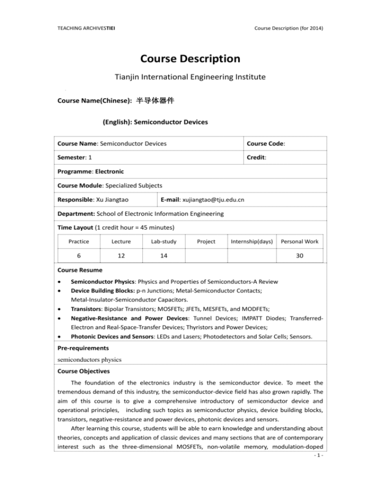
TEACHING ARCHIVESTIEI Course Description (for 2014) Course Description Tianjin International Engineering Institute Course Name(Chinese): 半导体器件 (English): Semiconductor Devices Course Name: Semiconductor Devices Course Code: Semester: 1 Credit: Programme: Electronic Course Module: Specialized Subjects Responsible: Xu Jiangtao E-mail: xujiangtao@tju.edu.cn Department: School of Electronic Information Engineering Time Layout (1 credit hour = 45 minutes) Practice Lecture Lab-study 6 12 14 Project Internship(days) Personal Work 30 Course Resume Semiconductor Physics: Physics and Properties of Semiconductors-A Review Device Building Blocks: p-n Junctions; Metal-Semiconductor Contacts; Metal-Insulator-Semiconductor Capacitors. Transistors: Bipolar Transistors; MOSFETs; JFETs, MESFETs, and MODFETs; Negative-Resistance and Power Devices: Tunnel Devices; IMPATT Diodes; TransferredElectron and Real-Space-Transfer Devices; Thyristors and Power Devices; Photonic Devices and Sensors: LEDs and Lasers; Photodetectors and Solar Cells; Sensors. Pre-requirements semiconductors physics Course Objectives The foundation of the electronics industry is the semiconductor device. To meet the tremendous demand of this industry, the semiconductor-device field has also grown rapidly. The aim of this course is to give a comprehensive introductory of semiconductor device and operational principles, including such topics as semiconductor physics, device building blocks, transistors, negative-resistance and power devices, photonic devices and sensors. After learning this course, students will be able to earn knowledge and understanding about theories, concepts and application of classic devices and many sections that are of contemporary interest such as the three-dimensional MOSFETs, non-volatile memory, modulation-doped -1- TEACHING ARCHIVESTIEI Course Description (for 2014) field-effect transistor, single-electron transistor, resonant-tunnelling diode, insulated-gate bipolar transistor, quantum cascade laser, semiconductor sensors. Course Syllabus 1. Introduction 2. Device Building Blocks 2.1 p-n Junctions 2.2 Metal-Semiconductor Contacts 2.3 Metal-Insulator-Semiconductor Capacitors. 3 .Transistors 3.1 Bipolar Transistors 3.2 MOSFETs 3.3 JFETs, MESFETs and MODFETs 4 .Negative-Resistance and Power Devices 4.1 Tunnel Devices 4.2 IMPATT Diodes 4.3Transferred-Electron and Real-Space-Transfer Devices 4.4 Thyristors and Power Devices 5 .Photonic Devices and Sensors 5.1 LEDs and Lasers 5.2 Photodetectors and Solar Cells 5.3 Sensors Text Book & References Required: S. M. Sze and Kwok K. Ng, Physics of Semiconductor Devices(3ed),WILEY. 2006 We may also use readings from a few textbooks: Ben G. Streetrnan, Sanjay Kumar Banerjee, Solid State Electronic Devices (6ed), PHI Learning. 2009 Robert F. pierret, Semiconductor device fundamentals, WILEY 1996 Chenming C. Hu ,Modern Semiconductor Devices for Integrated Circuits, Prentice Hall. 2010 Capability Tasks CT1 CT2 CT3 CT7 CT10 Achievements To understand the principle of operation of the PN junction, T. Bipolar and FET - Level: M To know the impact of physical and geometrical parameters on the performance - Level: A To design the basic circuits in MOS technology (ie reversers) - Level: A Students: Electronic year 1 -2-
