Handout
advertisement
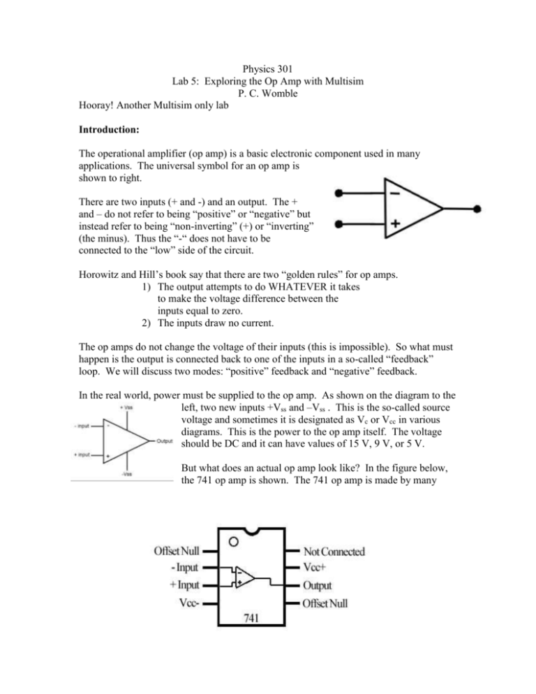
Physics 301 Lab 5: Exploring the Op Amp with Multisim P. C. Womble Hooray! Another Multisim only lab Introduction: The operational amplifier (op amp) is a basic electronic component used in many applications. The universal symbol for an op amp is shown to right. There are two inputs (+ and -) and an output. The + and – do not refer to being “positive” or “negative” but instead refer to being “non-inverting” (+) or “inverting” (the minus). Thus the “-“ does not have to be connected to the “low” side of the circuit. Horowitz and Hill’s book say that there are two “golden rules” for op amps. 1) The output attempts to do WHATEVER it takes to make the voltage difference between the inputs equal to zero. 2) The inputs draw no current. The op amps do not change the voltage of their inputs (this is impossible). So what must happen is the output is connected back to one of the inputs in a so-called “feedback” loop. We will discuss two modes: “positive” feedback and “negative” feedback. In the real world, power must be supplied to the op amp. As shown on the diagram to the left, two new inputs +Vss and –Vss . This is the so-called source voltage and sometimes it is designated as Vc or Vcc in various diagrams. This is the power to the op amp itself. The voltage should be DC and it can have values of 15 V, 9 V, or 5 V. But what does an actual op amp look like? In the figure below, the 741 op amp is shown. The 741 op amp is made by many manufacturers around the world. Any chip with designation of 741 has similar pin lay out. The biggest problem for a circuit designer is to determine the 1st pin. Pin 1 is found near the “notch” and a “dot” is often associated with it. Opposite pin 1 is pin 8. Thus the number scheme on the left side of the chip is 1 through 4 as you go away from the notch and 5 through 8 on the right side as you go up towards the notch. Schematics, like the figure showing the pin layouts, are available on the internet, particularly the manufacturers’ website. Circuit 1: V_In is a DC voltage source, U1 is a virtual op-amp with Vcc=15 V, Voltage_Out is a voltmeter with posivite lead connected to output of op-amp. Activity 1: 1. Set up Circuit 1 in Multisim. 2. Fill out Table 1 of the worksheet. 3. Using your favorite data analysis program, find a relationship between the Gain (V_Output/V_In) and the values of R1 and R2 (hint: examine the ratio with respect to R1). Attach any graphs to worksheet. 4. Finish filling out Table 2. Circuit 2: V_In is a DC voltage source, U1 is a virtual op-amp with Vcc=15 V, Voltage_Out is a voltmeter with posivite lead connected to output of op-amp. NOTE: The inverting input is connected to ground. Activity 2: 1. Set up Circuit 2 in Multisim. 2. Fill out Table 3 of the worksheet. 3. Using your favorite data analysis program, find a relationship between the Gain (V_Output/V_In) and the values of R1 and R2 (hint: examine the ratio with respect to R1). Attach any graphs to worksheet. Circuit 3: In this circuit, R1_1 must always equal R1_2 and R2_1 must always R2_1. Activity 3: 1. Set up Circuit 3 in Multsim 2. Fill out Table 4 in the worksheet. R2 (V2 V1 ) is a reasonable R1 relationship. Circuit 3 is called a “Difference Amplifier”. 4. Break the difference amplifier by violating the rules given in the caption as well as letting V2 equal to V1. Discuss in the worksheet. 3. From the data in Table 4, explore whether vout Circuit 4: Summing Amplifier Activity 4: 1. Set up Circuit 4 in Multisim. 2. Fill out Table 5 in the worksheet. 3. Explore whether the relationship R R R Vout V1 f V2 f V3 f R2 R3 R1 explains the data in Table 5 using a data analysis program.
