Origin of the ambipolar operation of a pentacene field
advertisement
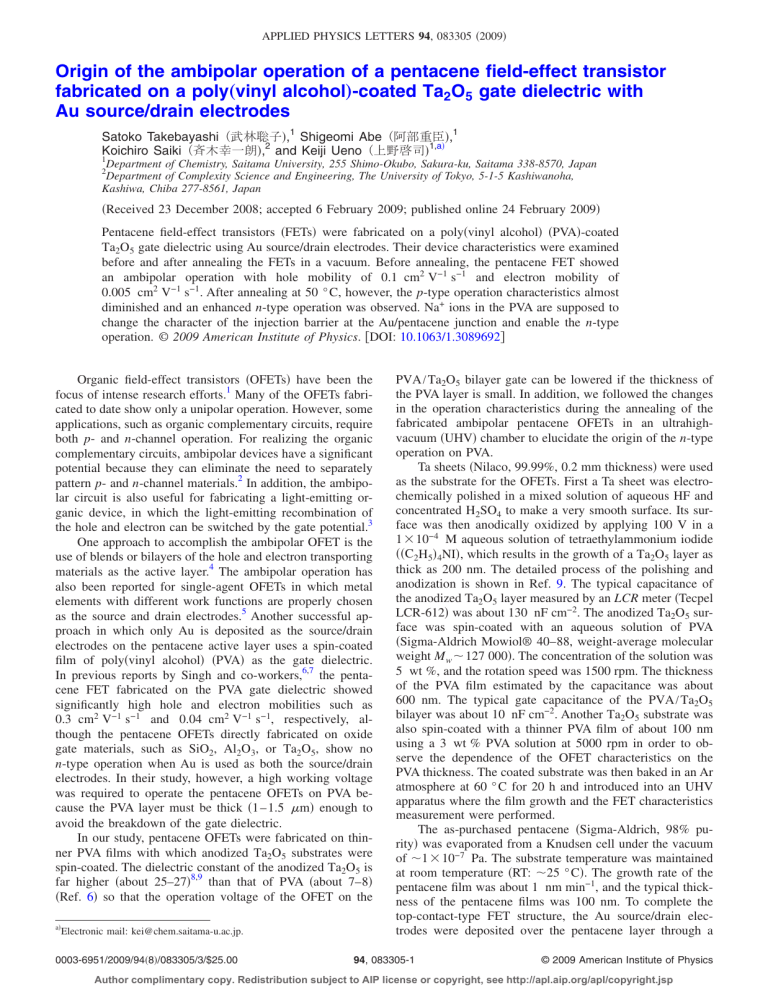
APPLIED PHYSICS LETTERS 94, 083305 共2009兲 Origin of the ambipolar operation of a pentacene field-effect transistor fabricated on a poly„vinyl alcohol…-coated Ta2O5 gate dielectric with Au source/drain electrodes Satoko Takebayashi (武林聡子兲,1 Shigeomi Abe (阿部重臣兲,1 Koichiro Saiki (斉木幸一朗兲,2 and Keiji Ueno (上野啓司兲1,a兲 1 Department of Chemistry, Saitama University, 255 Shimo-Okubo, Sakura-ku, Saitama 338-8570, Japan Department of Complexity Science and Engineering, The University of Tokyo, 5-1-5 Kashiwanoha, Kashiwa, Chiba 277-8561, Japan 2 共Received 23 December 2008; accepted 6 February 2009; published online 24 February 2009兲 Pentacene field-effect transistors 共FETs兲 were fabricated on a poly共vinyl alcohol兲 共PVA兲-coated Ta2O5 gate dielectric using Au source/drain electrodes. Their device characteristics were examined before and after annealing the FETs in a vacuum. Before annealing, the pentacene FET showed an ambipolar operation with hole mobility of 0.1 cm2 V−1 s−1 and electron mobility of 0.005 cm2 V−1 s−1. After annealing at 50 ° C, however, the p-type operation characteristics almost diminished and an enhanced n-type operation was observed. Na+ ions in the PVA are supposed to change the character of the injection barrier at the Au/pentacene junction and enable the n-type operation. © 2009 American Institute of Physics. 关DOI: 10.1063/1.3089692兴 Organic field-effect transistors 共OFETs兲 have been the focus of intense research efforts.1 Many of the OFETs fabricated to date show only a unipolar operation. However, some applications, such as organic complementary circuits, require both p- and n-channel operation. For realizing the organic complementary circuits, ambipolar devices have a significant potential because they can eliminate the need to separately pattern p- and n-channel materials.2 In addition, the ambipolar circuit is also useful for fabricating a light-emitting organic device, in which the light-emitting recombination of the hole and electron can be switched by the gate potential.3 One approach to accomplish the ambipolar OFET is the use of blends or bilayers of the hole and electron transporting materials as the active layer.4 The ambipolar operation has also been reported for single-agent OFETs in which metal elements with different work functions are properly chosen as the source and drain electrodes.5 Another successful approach in which only Au is deposited as the source/drain electrodes on the pentacene active layer uses a spin-coated film of poly共vinyl alcohol兲 共PVA兲 as the gate dielectric. In previous reports by Singh and co-workers,6,7 the pentacene FET fabricated on the PVA gate dielectric showed significantly high hole and electron mobilities such as 0.3 cm2 V−1 s−1 and 0.04 cm2 V−1 s−1, respectively, although the pentacene OFETs directly fabricated on oxide gate materials, such as SiO2, Al2O3, or Ta2O5, show no n-type operation when Au is used as both the source/drain electrodes. In their study, however, a high working voltage was required to operate the pentacene OFETs on PVA because the PVA layer must be thick 共1 – 1.5 m兲 enough to avoid the breakdown of the gate dielectric. In our study, pentacene OFETs were fabricated on thinner PVA films with which anodized Ta2O5 substrates were spin-coated. The dielectric constant of the anodized Ta2O5 is far higher 共about 25–27兲8,9 than that of PVA 共about 7–8兲 共Ref. 6兲 so that the operation voltage of the OFET on the a兲 Electronic mail: kei@chem.saitama-u.ac.jp. 0003-6951/2009/94共8兲/083305/3/$25.00 PVA/ Ta2O5 bilayer gate can be lowered if the thickness of the PVA layer is small. In addition, we followed the changes in the operation characteristics during the annealing of the fabricated ambipolar pentacene OFETs in an ultrahighvacuum 共UHV兲 chamber to elucidate the origin of the n-type operation on PVA. Ta sheets 共Nilaco, 99.99%, 0.2 mm thickness兲 were used as the substrate for the OFETs. First a Ta sheet was electrochemically polished in a mixed solution of aqueous HF and concentrated H2SO4 to make a very smooth surface. Its surface was then anodically oxidized by applying 100 V in a 1 ⫻ 10−4 M aqueous solution of tetraethylammonium iodide 共共C2H5兲4NI兲, which results in the growth of a Ta2O5 layer as thick as 200 nm. The detailed process of the polishing and anodization is shown in Ref. 9. The typical capacitance of the anodized Ta2O5 layer measured by an LCR meter 共Tecpel LCR-612兲 was about 130 nF cm−2. The anodized Ta2O5 surface was spin-coated with an aqueous solution of PVA 共Sigma-Aldrich Mowiol® 40–88, weight-average molecular weight M w ⬃ 127 000兲. The concentration of the solution was 5 wt %, and the rotation speed was 1500 rpm. The thickness of the PVA film estimated by the capacitance was about 600 nm. The typical gate capacitance of the PVA/ Ta2O5 bilayer was about 10 nF cm−2. Another Ta2O5 substrate was also spin-coated with a thinner PVA film of about 100 nm using a 3 wt % PVA solution at 5000 rpm in order to observe the dependence of the OFET characteristics on the PVA thickness. The coated substrate was then baked in an Ar atmosphere at 60 ° C for 20 h and introduced into an UHV apparatus where the film growth and the FET characteristics measurement were performed. The as-purchased pentacene 共Sigma-Aldrich, 98% purity兲 was evaporated from a Knudsen cell under the vacuum of ⬃1 ⫻ 10−7 Pa. The substrate temperature was maintained at room temperature 共RT: ⬃25 ° C兲. The growth rate of the pentacene film was about 1 nm min−1, and the typical thickness of the pentacene films was 100 nm. To complete the top-contact-type FET structure, the Au source/drain electrodes were deposited over the pentacene layer through a 94, 083305-1 © 2009 American Institute of Physics Author complimentary copy. Redistribution subject to AIP license or copyright, see http://apl.aip.org/apl/copyright.jsp 083305-2 Takebayashi et al. Appl. Phys. Lett. 94, 083305 共2009兲 FIG. 1. 共a兲 p-type and 共b兲 n-type output characteristics of a pentacene OFET fabricated on a Ta2O5 gate dielectric coated with a 600 nm PVA film measured before the thermal annealing. FIG. 2. 共a兲 p-type and 共b兲 n-type output characteristics of a pentacene OFET fabricated on a Ta2O5 gate dielectric coated with a 600 nm PVA film measured after the thermal annealing at 50 ° C for 18 h. shadow mask. The channel width and the channel length were 1 and 0.1 mm, respectively. Electrical characterization of the OFETs was performed in the UHV chamber without exposure to air using the combination of a Keithley 6517 A electrometer and a Keithley 487 picoammeter/voltage source. The measurements were performed at RT before and after annealing of the fabricated OFETs at 50 ° C for 18 h under UHV conditions. Pentacene films were also deposited on a PVA/ Ta2O5 bilayer at the substrate temperature of 50 ° C for 2 h. In this case, the pentacene film was thermally annealed before the deposition of the Au source/drain electrodes. Before the annealing, the pentacene OFETs fabricated at RT on the PVA共600 nm兲 / Ta2O5 bilayer gate dielectric showed the usual p-type operation, and the n-type operation was also observed when a high positive gate voltage 共VG兲 was applied. Figure 1 shows the p-channel and n-channel operations of the ambipolar pentacene OFET. In the ambipolar OFET, increasing the drain voltage 共VD兲 above a certain value, which is gate bias dependent, results in a characteristic increase in the drain current 共ID兲 when the absolute value of VG 共兩VG兩兲 is low. For the present output characteristics of the p-type operation shown in Fig. 1共a兲, such an increase in ID is barely observed only at VG = 0 V. For the output characteristics of the n-type operation shown in Fig. 1共b兲, however, a steep increase in ID, which is due to the hole injection from the drain electrode, is observed in the increased VD region for a 兩VG兩 lower than 80 V. For the higher 兩VG兩, the device shows an enhanced ID and exhibits a normal n-type operation with the saturated regions. The hole and electron mobilities calculated from the transfer characteristics in the saturated regions using the theoretical equation1 are 0.1 and 0.005 cm2 V−1 s−1, respectively. The observed hole mobility of the pentacene OFET on the PVA/ Ta2O5 bilayer is comparable to that of the OFET fabricated on a bare SiO2 or Ta2O5 gate using the same pentacene source and UHV apparatus, although the n-type operation was never observed on the bare oxide surfaces. After the annealing of this sample, the operating characteristics showed drastic changes. Figure 2 shows the p-channel and n-channel operations after the annealing at 50 ° C for 18 h. In the annealed OFET, the ID of the p-type operation is heavily reduced. In addition, a steep increase in ID, which is due to the electron injection from the drain electrode, is observed in the increased VD region for the low 兩VG兩 as shown in Fig. 2共a兲. The hole mobility of the annealed OFET is calculated to be 0.0008 cm2 V−1 s−1. In contrast, the n-type operation is fairly improved after the annealing. As shown in Fig. 2共b兲, a six times larger ID is observed at VD = 100 V and VG = 100 V. The electron mobility of the annealed OFET was calculated to be 0.006 cm2 V−1 s−1. When we deposited the pentacene film on the PVA/ Ta2O5 gate dielectric at 50 ° C, similar p- and n-type performances were observed compared with those measured before the annealing of the OFET fabricated at RT. This result indicates that only the annealing after the deposition of the source/drain Au electrodes changes the performance of the OFET on the PVA/ Ta2O5 bilayer gate dielectric. The OFETs were also fabricated on a 100 nm PVA/ Ta2O5 bilayer gate dielectric because a thinner PVA coating is favorable for the low-voltage operation. The n-type operation, however, could not be observed on the thinner PVA film, and only the usual p-type unipolar characteristics were observed before and even after the annealing. Here, it must be considered that the PVA reagent is synthesized from poly共vinyl acetate兲 by the saponification with sodium hydroxide so that it contains Na impurity. In reality, a preliminary quantitative analysis by inductively coupled plasma spectrometry has revealed that a 5 wt % aqueous solution of PVA includes 7 ppm Na by weight. It is known that alkali metal elements have small work functions and change the barrier height against the electron injection from the cathode into the active layer of an organic light-emitting device.10 It is also reported that the pentacene OFET using Ca as the source/drain electrodes shows the ambipolar operation due to its small work function.5 It was also observed in our preliminary experiments that the doping of Li into the pentacene active layer at RT never caused the n-type operation, but the usual p-type operation was still observed. Therefore, we postulate that the Na impurity in the PVA film changes the condition of the junctions at the Au/ pentacene interface during annealing of the fabricated OFETs. The behavior of the Na impurity is schematically shown in Fig. 3. During the deposition of the evaporated “hot” Au atoms onto the pentacene/PVA surface, warmed Na+ ions existing in the PVA film 关Fig. 3共a兲兴 are allowed to diffuse. Some of them might intrude into the pentacene film FIG. 3. Schematic view of the diffusion of Na+ ions from a PVA film to Au/pentacene interface. 共a兲 Before and 共b兲 after the deposition of Au electrodes. 共c兲 After the successive thermal annealing of a fabricated OFET. Author complimentary copy. Redistribution subject to AIP license or copyright, see http://apl.aip.org/apl/copyright.jsp 083305-3 Appl. Phys. Lett. 94, 083305 共2009兲 Takebayashi et al. FIG. 4. 共a兲 p-type and 共b兲 n-type output characteristics of a pentacene OFET fabricated on a Ta2O5 gate dielectric coated with a thinner 共350 nm兲 PVA film including a higher concentration of a Na+ impurity 共700 ppm兲 measured before the thermal annealing. and reach the Au/pentacene interface, as shown in Fig. 3共b兲. Such Na+ ions reduce the work function of the source/drain electrodes, which is favorable for the electron injection but unfavorable for the hole injection into the pentacene channel. The just fabricated OFETs then show the ambipolar operation due to the limited change of the injection condition. Further annealing of the OFETs promotes the diffusion of Na+ ions so that the injection condition is almost fully changed, as shown in Fig. 3共c兲. Then the OFETs show improved n-type and deteriorated p-type operation characteristics. Therefore, annealing of the sample during the deposition of the pentacene film, namely, before the deposition of Au electrodes, has no direct effect on the change in the injection condition. The annealing only after the deposition of Au electrodes can gather the Na+ ions at the Au/pentacene interface and change the injection condition. If the PVA film is too thin, the total amount of Na+ ions becomes insufficient for changing the work function of the source/drain electrodes. The ambipolar operation might be observed on the thinner PVA film if a higher positive VG was applied, but it usually causes a breakdown of the PVA/ Ta2O5 gate. Then, we tried to add excess Na+ ions to the PVA film. If the concentration of Na+ is higher, it is expected that the ambipolar operation also occurs on a thinner PVA film. We added an aqueous NaOH solution to the 5 wt % aqueous PVA solution and prepared a solution including 700 ppm Na+ by weight. Next, the 200 nm thick Ta2O5 was spin-coated with this PVA solution at 2000 rpm, which results in a 350 nm thick Na+-rich PVA film. Figure 4 shows the output characteristics of a pentacene OFET that was fabricated on this thinner PVA/ Ta2O5 bilayer gate and not annealed before the electric measurement. Although the PVA film is thinner, this OFET shows the ambipolar opera- tion. The calculated hole and electron mobilities of the present OFET are 0.47 and 0.03 cm2 V−1 s−1, respectively. In addition, the thinner PVA film makes it possible to operate the ambipolar OFET with lower bias voltages. In the p-type operation region of the previous OFET shown in Fig. 1共a兲, the ID of −2.0 A was obtained with VD = −20 V and VG = −10 V. However, in the present OFET shown in Fig. 4共a兲, the same ID flows with VD = −15 V and VG = −10 V. In the n-type operation region of the previous OFET shown in Fig. 1共b兲, the ID of 0.3 A was obtained with VD = 100 V and VG = 100 V. In the present OFET shown in Fig. 4共b兲, the same ID flows with VD = 10 V and VG = 100 V. Therefore, it is concluded that the addition of the Na+ impurity is effective for decreasing the PVA film thickness and reducing the operating voltage of the ambipolar pentacene OFET. In summary, the pentacene OFETs were fabricated on the PVA-coated Ta2O5 gate dielectric using Au source/drain electrodes. The as-fabricated pentacene OFETs showed an ambipolar operation, but the p-type operation character almost diminished, and an enhanced n-type operation was observed after the annealing in a vacuum. Na+ ions in the PVA are supposed to change the character of the injection barrier at the Au/pentacene junction and enable the n-type operation. This work was supported by a Grant-in-Aid for Creative Scientific Research 共Grant No. 14GS0207兲 from the Ministry of Education, Culture, Sports, Science and Technology of Japan. C. D. Dimitrakopoulos and P. R. L. Malenfant, Adv. Mater. 共Weinheim, Ger.兲 14, 99 共2002兲. 2 B. K. Crone, A. Dodabalapur, R. Sarpeshkar, R. W. Filas, Y.-Y. Lin, Z. Bao, J. H. O’Neill, W. Li, and H. E. Katz, J. Appl. Phys. 89, 5125 共2001兲. 3 A. Hepp, H. Heil, W. Weise, M. Ahles, R. Schmechel, and H. von Seggern, Phys. Rev. Lett. 91, 157406 共2003兲. 4 A. Dodabalapur, H. E. Katz, L. Torsi, and R. C. Haddon, Science 269, 1560 共1995兲. 5 T. Yasuda, T. Goto, K. Fujita, and T. Tsutsui, Appl. Phys. Lett. 85, 2098 共2004兲. 6 Th. B. Singh, F. Meghdadi, S. Günes, N. Marjanovic, G. Horowitz, P. Lang, S. Bauer, and N. S. Sariciftci, Adv. Mater. 共Weinheim, Ger.兲 17, 2315 共2005兲. 7 Th. B. Singh, P. Senkarabacak, N. S. Sariciftci, A. Tanda, C. Lackner, R. Hagelauer, and G. Horowitz, Appl. Phys. Lett. 89, 033512 共2006兲. 8 J. J. Randall, Jr., W. J. Bernard, and R. R. Wilkinson, Electrochim. Acta 10, 183 共1965兲. 9 K. Ueno, S. Abe, R. Onoki, and K. Saiki, J. Appl. Phys. 98, 114503 共2005兲. 10 L. S. Hung, C. W. Tang, and M. G. Mason, Appl. Phys. Lett. 70, 152 共1997兲. 1 Author complimentary copy. Redistribution subject to AIP license or copyright, see http://apl.aip.org/apl/copyright.jsp
