1 E84 Lecture 3/26/14 K. Candler Agenda o Semiconductor
advertisement
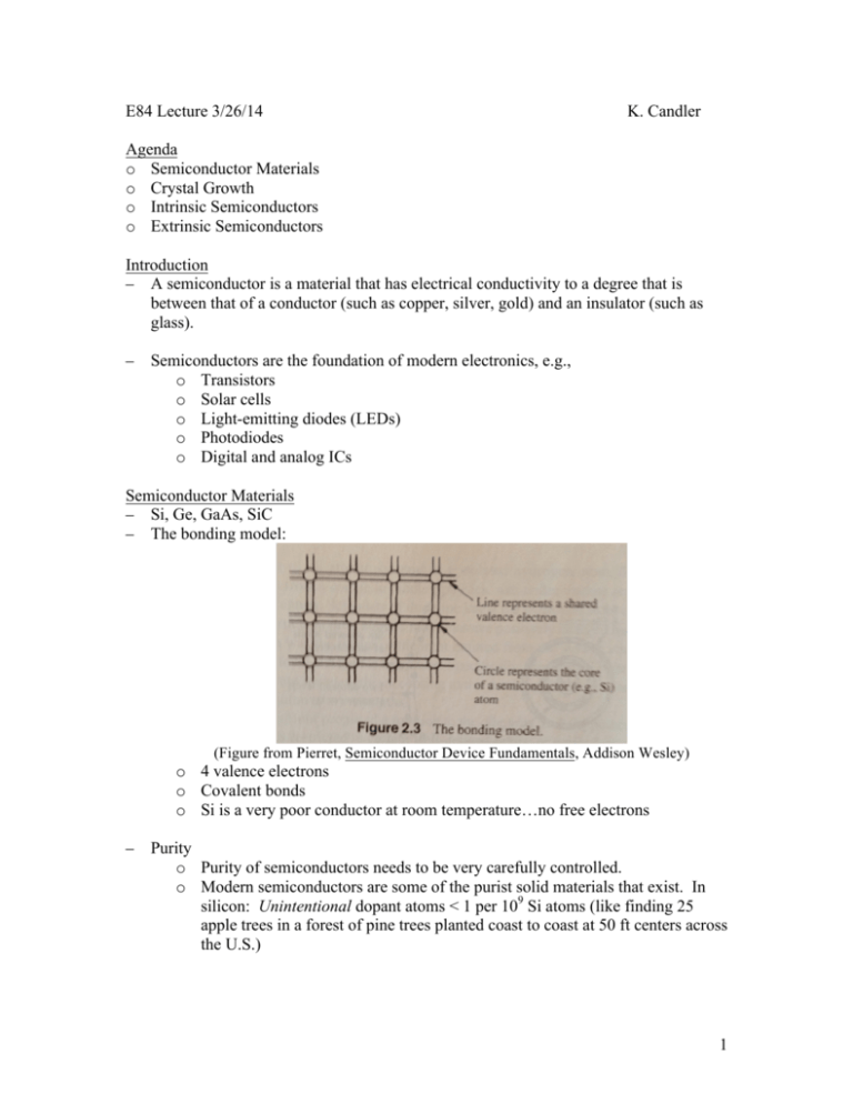
E84 Lecture 3/26/14 K. Candler Agenda o Semiconductor Materials o Crystal Growth o Intrinsic Semiconductors o Extrinsic Semiconductors Introduction – A semiconductor is a material that has electrical conductivity to a degree that is between that of a conductor (such as copper, silver, gold) and an insulator (such as glass). – Semiconductors are the foundation of modern electronics, e.g., o Transistors o Solar cells o Light-emitting diodes (LEDs) o Photodiodes o Digital and analog ICs Semiconductor Materials – Si, Ge, GaAs, SiC – The bonding model: (Figure from Pierret, Semiconductor Device Fundamentals, Addison Wesley) o 4 valence electrons o Covalent bonds o Si is a very poor conductor at room temperature…no free electrons – Purity o Purity of semiconductors needs to be very carefully controlled. o Modern semiconductors are some of the purist solid materials that exist. In silicon: Unintentional dopant atoms < 1 per 109 Si atoms (like finding 25 apple trees in a forest of pine trees planted coast to coast at 50 ft centers across the U.S.) 1 – Structure Amorphous Polycrystalline Crystalline (Figure from Pierret, Semiconductor Device Fundamentals, Addison Wesley) o Amorphous: No recognizable long-range order o Polycrystalline: Completely ordered in segments o Crystalline: Entire solid is made up of atoms in orderly array Crystal Growth – Obtaining Ultrapure Polycrystalline Si (Figure from Pierret, Semiconductor Device Fundamentals, Addison Wesley) – Obtaining Single-Crystal Si o Invented in 1916 by a Polish scientist, Jan Czochralski o A seed crystal is dipped into a crucible of molten silicon and withdrawn slowly, pulling a cylindrical single crystal as the silicon crystallizes on the seed. o Show video (up to 4 min mark): http://www.youtube.com/watch?v=aWVywhzuHnQ Intrinsic Semiconductors – No impurities and lattice defects in its crystal structure – If an electron gains enough energy (from thermal or optical excitation), it can break the covalent bond and become a free carrier. o E > Eg ; Eg = bandgap energy (the energy needed for an electron to break a bond) Eg = 1.12 eV (Si) Eg = 1.42 eV (GaAs) 2 – Eg = 0.66 eV (Ge) Eg (metal) << Eg (semiconductor) << Eg (insulator) When a bond is broken, two mobile charge carriers are created: electrons (negative charge) and holes (positive charge) (Figure from Howe & Sodini, Microelectronics, Prentice Hall) – – – – no = po ≡ ni (at thermal equilibrium) o no = electron concentration at thermal equilibrium [cm-3] o po = hole concentration at thermal equilibrium [cm-3] o ni = intrinsic carrier concentration (ni = 1.5 x 1010 cm-3 in Si at T = 300 K) Exercise: How many bonds are broken in Si at room temperature? (Hint: silicon atom density = 5 x 10²² Si atoms/cm3) o Total possible bonds = 5 x 10²² Si atoms/cm-3 x 4 bonds/atom = 2 x 10²³ bonds/cm-3 o # broken bonds at room temp = ni = 1.5 x 1010 cm-3 o # broken bonds/total possible bonds = 1.5 x 10¹⁰/2 x 1023 ~ 0.7 x 10⁻¹³ less than one bond in 1013 is broken in Si at room temperature! Main point: At room temperature, relatively few electrons gain enough energy to become free electrons, the overall conductivity of semiconductors is low, thereby their name semiconductors. Increasing temperature leads to better or worse conductivity? Extrinsic Semiconductors – Contain impurity atoms, which contribute extra electrons and holes (improve conductivity) – Impurities are introduced through doping. – Dopants are Group III (B, Ga, In, Al) or V (P, As, Sb). – Doping with Group V Elements (Donors) 3 (Figure from Pierret, Semiconductor Device Fundamentals, Addison Wesley) – Extra electrons: N-type semiconductor Majority carrier: electron Minority carrier: hole Doping with Group III Elements (Acceptors): (Figure from Pierret, Semiconductor Device Fundamentals, Addison Wesley) – Extra holes: P-type semiconductor Majority carrier: hole Minority carrier: electron How to calculate # electrons and holes (mobile carriers) in doped Si? o Mass Action Law: n o ⋅ po = n i 2 o rate of electron-hole pair generation = rate of recombination no charge buildup inside Si in thermal equilibrium (no heat flow) o N-type case no ≅ N d po = ni2 no (one electron per donor) = ni2 Nd 4 o P-type case (one hole per donor) po ≅ N a no = ni2 po = ni2 Na o Example: A silicon sample is doped with 1017 As atoms per cm3. What are the carrier concentrations in the Si sample at 300 K? As is n-type, Nd = 1017 cm-3 - no = Nd = 1017 cm-3 - po = ni2/ no = 1020/1017 = 103 cm-3 o Main point: The majority carriers outnumber the minority carriers by many orders of magnitude! 5
