22. analog inputs and outputs
advertisement
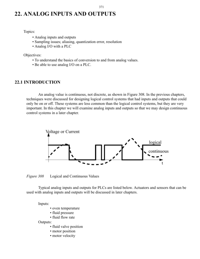
371 22. ANALOG INPUTS AND OUTPUTS Topics: • Analog inputs and outputs • Sampling issues; aliasing, quantization error, resolution • Analog I/O with a PLC Objectives: • To understand the basics of conversion to and from analog values. • Be able to use analog I/O on a PLC. 22.1 INTRODUCTION An analog value is continuous, not discrete, as shown in Figure 308. In the previous chapters, techniques were discussed for designing logical control systems that had inputs and outputs that could only be on or off. These systems are less common than the logical control systems, but they are very important. In this chapter we will examine analog inputs and outputs so that we may design continuous control systems in a later chapter. Voltage or Current logical continuous t Figure 308 Logical and Continuous Values Typical analog inputs and outputs for PLCs are listed below. Actuators and sensors that can be used with analog inputs and outputs will be discussed in later chapters. Inputs: • oven temperature • fluid pressure • fluid flow rate Outputs: • fluid valve position • motor position • motor velocity 372 This chapter will focus on the general principles behind digital-to-analog (D/A) and analog-todigital (A/D) conversion. The chapter will show how to output and input analog values with a PLC. 22.2 ANALOG INPUTS To input an analog voltage (into a PLC or any other computer) the continuous voltage value must be sampled and then converted to a numerical value by an A/D converter. Figure 309 shows a continuous voltage changing over time. There are three samples shown on the figure. The process of sampling the data is not instantaneous, so each sample has a start and stop time. The time required to acquire the sample is called the sampling time. A/D converters can only acquire a limited number of samples per second. The time between samples is called the sampling period T, and the inverse of the sampling period is the sampling frequency (also called sampling rate). The sampling time is often much smaller than the sampling period. The sampling frequency is specified when buying hardware, but for a PLC a maximum sampling rate might be 20Hz. Voltage is sampled during these time periods voltage time T = (Sampling Frequency)-1 Figure 309 Sampling time Sampling an Analog Voltage A more realistic drawing of sampled data is shown in Figure 310. This data is noisier, and even between the start and end of the data sample there is a significant change in the voltage value. The data value sampled will be somewhere between the voltage at the start and end of the sample. The maximum (Vmax) and minimum (Vmin) voltages are a function of the control hardware. These are often specified when purchasing hardware, but reasonable ranges are; 0V to 5V 0V to 10V -5V to 5V -10V to 10V 373 The number of bits of the A/D converter is the number of bits in the result word. If the A/D converter is 8 bit then the result can read up to 256 different voltage levels. Most A/D converters have 12 bits, 16 bit converters are used for precision measurements. V(t) V max V ( t2 ) V ( t1 ) V min t τ t1 t2 where, V ( t ) = the actual voltage over time τ = sample interval for A/D converter t = time t 1, t 2 = time at start,end of sample V ( t 1 ), V ( t 2 ) = voltage at start, end of sample V min, V max = input voltage range of A/D converter N = number of bits in the A/D converter Figure 310 Parameters for an A/D Conversion The parameters defined in Figure 310 can be used to calculate values for A/D converters. These equations are summarized in Figure 311. Equation 1 relates the number of bits of an A/D converter to the resolution. In a normal A/D converter the minimum range value, Rmin, is zero, however some devices will provide 2’s compliment negative numbers for negative voltages. Equation 2 gives the error that can be expected with an A/D converter given the range between the minimum and maximum voltages, and the resolution (this is commonly called the quantization error). Equation 3 relates the voltage range and resolution to the voltage input to estimate the integer that the A/D converter will record. Finally, equation 4 allows a conversion between the integer value from the A/D converter, and a voltage in the computer. 374 R = 2 N = R max – R min V max – V min V ERROR = ⎛ -----------------------------⎞ ⎝ ⎠ 2R (1) (2) V in – V min V I = INT ⎛ -----------------------------⎞ ( R – 1 ) + R min ⎝ V max – V min⎠ (3) V I – R min V C = ⎛ ----------------------⎞ ( V max – V min ) + V min ⎝ (R – 1) ⎠ (4) where, R, R min, R max = absolute and relative resolution of A/D converter V I = the integer value representing the input voltage V C = the voltage calculated from the integer value V ERROR = the maximum quantization error Figure 311 A/D Converter Equations Consider a simple example, a 10 bit A/D converter can read voltages between -10V and 10V. This gives a resolution of 1024, where 0 is -10V and 1023 is +10V. Because there are only 1024 steps there is a maximum error of ±9.8mV. If a voltage of 4.564V is input into the PLC, the A/D converter converts the voltage to an integer value of 745. When we convert this back to a voltage the result is 4.565V. The resulting quantization error is 4.565V-4.564V=+0.001V. This error can be reduced by selecting an A/D converter with more bits. Each bit halves the quantization error. 375 Given, N = 10, R min = 0 V max = 10V V min = – 10V V in = 4.564V Calculate, R = R max = 2 N = 1024 V max – V min V ERROR = ⎛⎝ -----------------------------⎞⎠ = 0.0098V 2R V in – V min V I = INT ⎛ -----------------------------⎞ ( R – 1 ) + 0 = 745 ⎝ V max – V min⎠ VI – 0 V C = ⎛ --------------⎞ ( V max – V min ) + V min = 4.565V ⎝ R – 1⎠ Figure 312 Sample Calculation of A/D Values If the voltage being sampled is changing too fast we may get false readings, as shown in Figure 313. In the upper graph the waveform completes seven cycles, and 9 samples are taken. The bottom graph plots out the values read. The sampling frequency was too low, so the signal read appears to be different that it actually is, this is called aliasing. Figure 313 Low Sampling Frequencies Cause Aliasing 376 The Nyquist criterion specifies that sampling frequencies should be at least twice the frequency of the signal being measured, otherwise aliasing will occur. The example in Figure 313 violated this principle, so the signal was aliased. If this happens in real applications the process will appear to operate erratically. In practice the sample frequency should be 4 or more times faster than the system frequency. f AD > 2f signal where, f AD = sampling frequency f signal = maximum frequency of the input There are other practical details that should be considered when designing applications with analog inputs; • Noise - Since the sampling window for a signal is short, noise will have added effect on the signal read. For example, a momentary voltage spike might result in a higher than normal reading. Shielded data cables are commonly used to reduce the noise levels. • Delay - When the sample is requested, a short period of time passes before the final sample value is obtained. • Multiplexing - Most analog input cards allow multiple inputs. These may share the A/D converter using a technique called multiplexing. If there are 4 channels using an A/D converter with a maximum sampling rate of 100Hz, the maximum sampling rate per channel is 25Hz. • Signal Conditioners - Signal conditioners are used to amplify, or filter signals coming from transducers, before they are read by the A/D converter. • Resistance - A/D converters normally have high input impedance (resistance), so they do not affect circuits they are measuring. • Single Ended Inputs - Voltage inputs to a PLC can use a single common for multiple inputs, these types of inputs are called single ended inputs. These tend to be more prone to noise. • Double Ended Inputs - Each double ended input has its own common. This reduces problems with electrical noise, but also tends to reduce the number of inputs by half. 377 ASIDE: This device is an 8 bit A/D converter. The main concept behind this is the successive approximation logic. Once the reset is toggled the converter will start by setting the most significant bit of the 8 bit number. This will be converted to a voltage Ve that is a function of the +/-Vref values. The value of Ve is compared to Vin and a simple logic check determines which is larger. If the value of Ve is larger the bit is turned off. The logic then repeats similar steps from the most to least significant bits. Once the last bit has been set on/off and checked the conversion will be complete, and a done bit can be set to indicate a valid conversion value. Vin above (+ve) or below (-ve) Ve Vin + - +Vref clock successive approximation logic 8 D to A converter Ve reset done 8 -Vref data out Quite often an A/D converter will multiplex between various inputs. As it switches the voltage will be sampled by a sample and hold circuit. This will then be converted to a digital value. The sample and hold circuits can be used before the multiplexer to collect data values at the same instant in time. Figure 314 A Successive Approximation A/D Converter 22.3 ANALOG OUTPUTS Analog outputs are much simpler than analog inputs. To set an analog output an integer is converted to a voltage. This process is very fast, and does not experience the timing problems with analog inputs. But, analog outputs are subject to quantization errors. Figure 315 gives a summary of the important relationships. These relationships are almost identical to those of the A/D converter. 378 R = 2 N (5) = R max – R min V max – V min V ERROR = ⎛ -----------------------------⎞ ⎝ ⎠ 2R (6) V desired – V min V I = INT ⎛⎝ -----------------------------------⎞⎠ ( R – 1 ) + R min V max – V min (7) V I – R min V output = ⎛ ----------------------⎞ ( V max – V min ) + V min ⎝ (R – 1) ⎠ (8) where, R, R min, R max = absolute and relative resolution of A/D converter V ERROR = the maximum quantization error V I = the integer value representing the desired voltage V output = the voltage output using the integer value V desired = the desired analog output value Figure 315 Analog Output Relationships Assume we are using an 8 bit D/A converter that outputs values between 0V and 10V. We have a resolution of 256, where 0 results in an output of 0V and 255 results in 10V. The quantization error will be 20mV. If we want to output a voltage of 6.234V, we would specify an output integer of 159, this would result in an output voltage of 6.235V. The quantization error would be 6.235V-6.234V=0.001V. Given, N = 8, R min = 0 V max = 10V V min = 0V V desired = 6.234V Calculate, R = R max = 2 N = 256 V max – V min V ERROR = ⎛ -----------------------------⎞ = 0.020V ⎝ ⎠ 2R V in – V min V I = INT ⎛ -----------------------------⎞ ( R – 1 ) + 0 = 159 ⎝ V max – V min⎠ VI – 0 V C = ⎛⎝ --------------⎞⎠ ( V max – V min ) + V min = 6.235V R–1 379 The current output from a D/A converter is normally limited to a small value, typically less than 20mA. This is enough for instrumentation, but for high current loads, such as motors, a current amplifier is needed. This type of interface will be discussed later. If the current limit is exceeded for 5V output, the voltage will decrease (so don’t exceed the rated voltage). If the current limit is exceeded for long periods of time the D/A output may be damaged. ASIDE: 5KΩ MSB bit 3 bit 2 10KΩ 20KΩ V– V + LSB bit 0 + + 0 Computer bit 1 V ss Vo 40KΩ 80KΩ First we write the obvious, V + = 0 = V– Next, sum the currents into the inverting input as a function of the output voltage and the input voltages from the computer, V b2 V b1 V b0 V b3 Vo -------------- + -------------- + -------------- + -------------- = ----------10KΩ 20KΩ 40KΩ 80KΩ 5KΩ ∴V o = 0.5V b 3 + 0.25V b2 + 0.125V b 1 + 0.0625V b0 Consider an example where the binary output is 1110, with 5V for on, ∴V o = 0.5 ( 5V ) + 0.25 ( 5V ) + 0.125 ( 5V ) + 0.625 ( 0V ) = 4.375V Figure 316 A Digital-To-Analog Converter 22.4 ANALOG INPUTS AND OUTPUTS WITH CONTROLLOGIX In this section analog I/O will be discussed using a 1794-IE4XOE2/B 4 Input/2Output 24V DC Non-Isolated Analog module. The card has a 12 bit resolution. To use this module it is defined under the ’I/O Configuration’. While configuring the module the following options are available. 380 • Update rate (Requested Packet Interval) 2-750ms • Input channel ranges for channels 0 to 3 4 to 20mA 0 to 10V/0 to 20mV -10 to 10V • Output channel ranges for channel 0 and 1 4 to 20mA 0 to 10V/0 to 20mV -10 to 10V After the card is configured the configuration words are available in the ’controller scooped tags’. These are listed below with descriptions assuming the card is in ’rack:2:’. The configuration words may also be used to update the card during operation. To do this the values are changed using normal program statements to read or write to values. rack:2:C.Ch0SafeStateConfig - Sets the safe state when the module update fails rack:2:C.Ch1SafeStateConfig - Sets the safe state when the module update fails rack:2:C.Ch0InputFullRange - 0 = 4-20mA; 1 = -10-10V,0-10V,0-20mA rack:2:C.Ch1InputFullRange - 0 = 4-20mA; 1 = -10-10V,0-10V,0-20mA rack:2:C.Ch2InputFullRange - 0 = 4-20mA; 1 = -10-10V,0-10V,0-20mA rack:2:C.Ch3InputFullRange - 0 = 4-20mA; 1 = -10-10V,0-10V,0-20mA rack:2:C.Ch0OututFullRange - 0 = 4-20mA; 1 = -10-10V,0-10V,0-20mA rack:2:C.Ch1OutputFullRange - 0 = 4-20mA; 1 = -10-10V,0-10V,0-20mA rack:2:C.Ch0InputConfigSelect - 0 = 0-10V, 0-20mA; 1 = 4-20mA, -10V-10V rack:2:C.Ch1InputConfigSelect - 0 = 0-10V, 0-20mA; 1 = 4-20mA, -10V-10V rack:2:C.Ch2InputConfigSelect - 0 = 0-10V, 0-20mA; 1 = 4-20mA, -10V-10V rack:2:C.Ch3InputConfigSelect - 0 = 0-10V, 0-20mA; 1 = 4-20mA, -10V-10V rack:2:C.Ch0OutputConfigSelect - 0 = 0-10V, 0-20mA; 1 = 4-20mA, -10V-10V rack:2:C.Ch1OutputConfigSelect - 0 = 0-10V, 0-20mA; 1 = 4-20mA, -10V-10V rack:2:C.SSCh0OutputData - A safe output value for channel 0 rack:2:C.SSCh1OutputData - A safe output value for channel 1 rack:2:I.Fault - Returns a fault code for the module rack:2:I.Ch0InputData - The analog input value read on channel 0 rack:2:I.Ch1InputData - The analog input value read on channel 1 rack:2:I.Ch2InputData - The analog input value read on channel 2 rack:2:I.Ch3InputData - The analog input value read on channel 3 rack:2:I.Ch0InputUnderrange - The channel 0 current is below 4mA rack:2:I.Ch1InputUnderrange - The channel 1 current is below 4mA rack:2:I.Ch2InputUnderrange - The channel 2 current is below 4mA rack:2:I.Ch3InputUnderrange - The channel 3 current is below 4mA rack:2:I.Ch0OutputOpenWire - The output current is zero - indicates broken wire rack:2:I.Ch1OutputOpenWire - The output current is zero - indicates broken wire rack:2:I.PowerUp - The module is configured and running normally rack:2:O.Ch0OutputData - The analog output voltage for channel 0 rack:2:O.Ch1OutputData - The analog output voltage for channel 1 Figure 317 shows a simple analog IO example with some error checking. The system uses start and stop buttons to operate, along with a check for module errors. If the system is running the input 381 voltage from input channel 0 will be divided by two and then set as the output voltage for output channel 0. If the system is not running the output voltage on channel zero is set to 0 (0V). start run stop EQU 0 rack:2:I.Fault run run CPT Dest: rack:2:O.Ch0OutputData Exp.: "rack:2:I.Ch0InputData / 2" run MOV 0 rack:2:O.Ch0OutputData Figure 317 A Voltage Divide by Two Example Although the card is a 12 bit card, it uses data values as if it has 15 digits of accuracy. Hence the valid range for the card is -32,768 to 32,767. 22.4.1 ANALOG INPUTS AND OUTPUTS WITH A PLC-5 (NOTE: This section is optional but is included for historical perspective.) The PLC 5 ladder logic in Figure 318 will control an analog input card. The Block Transfer Write (BTW) statement will send configuration data from integer memory to the analog card in rack 0, slot 0. The data from N7:30 to N7:66 describes the configuration for different input channels. Once the analog input card receives this it will start doing analog conversions. The instruction is edge triggered, so it is run with the first scan, but the input is turned off while it is active, BT10:0/EN. This instruction will require multiple scans before all of the data has been written to the card. The update input is only needed if the configuration for the input changes, but this would be unusual. The Block Transfer Read (BTR) will retrieve data from the card and store it in memory N7:10 to N7:29. This data will contain the analog input values. The function is edge triggered, so the enable bits prevent it from trying to read data before the card is configured BT10:0/EN. The BT10:1/EN bit will prevent if from starting another read until the previous one is complete. Without these the instructions experience continuous errors. The MOV instruction will move the data value from one analog input to another memory location when the BTR instruction is done. 382 update BT10:0/EN S2:1/15 BT10:0/EN BT10:1/DN BT10:1/EN BTW Rack: 0 Group: 0 Module: 0 BT Array: BT10:0 Data File: N7:30 Length: 37 Continuous: no BTR Rack: 0 Group: 0 Module: 0 BT Array: BT10:1 Data File: N7:10 Length: 20 Continuous: no MOV Source N7:15 Dest N7:0 note: analog channel #2 Note: The basic operation is that the BTW will send the control block to the input card. The inputs are used because the BTR and BTW commands may take longer than one scan. Figure 318 Ladder Logic to Control an Analog Input Card The data to configure a 1771-IFE Analog Input Card is shown in Figure 319. (Note: each type of card will be different, and you need to refer to the manuals for this information.) The 1771-IFE is a 12 bit card, so the range will have up to 2**12 = 4096 values. The card can have 8 double ended inputs, or 16 single ended inputs (these are set with jumpers on the board). To configure the card a total of 37 data words are needed. The voltage range of different inputs are set using the bits in word 0 (N7:30) and 1 (N7:31). For example, to set the voltage range on channel 10 to -5V to 5V we would need to set the bits, N7:31/3 = 1 and N7:31/2 = 0. Bits in data word 2 (N7:32) are set to determine the general configuration of the card. For example, if word 2 was 0001 0100 0000 0000b the card would be set for; a delay of 00010 between samples, to return 2s compliment results, using single ended inputs, and no filtering. The remaining data words, from 3 to 36, allow data values to be scaled to a new range. Words 3 and 4 are for channel 1, words 5 and 6 are for channels 2 and so on. To scale the data, the new minimum value is put in the first word (word 3 for channel 1), and the maximum value is put in the second word (word 4 for channel 1). The card then automatically converts the actual data reading between 0 and 4095 to the new data range indicated in word 3 and 4. One oddity of this card is that the data values for scaling must always be BCD, regardless of the data type setting. The manual for this card claims that putting zeros in the scaling values will cause the card to leave the data unscaled, but in practice it is better to enter values of 0 for the minimum and 4095 for the maximum. 383 N7:30 0 R8 R1 R1 1 2 3 4 5 6 R16 R16 R15 R15 R14 R14 R13 R13 R12 R12 R11 R11 R10 R10 R9 R9 S F R8 S R7 S R7 S R6 S R6 N R5 N R5 R4 T F L1 U1 L2 U2 33 34 L15 U15 35 36 L16 U16 R1,R2,...R16 - range values 00 01 10 11 R4 F R3 F R3 F R2 F R2 F F 1 to 5V 0 to 5V -5 to 5V -10 to 10V T - input type - (0) gives single ended, (1) gives double ended N - data format - 00 01 10 11 BCD not used 2’s complement binary signed magnitude binary F - filter function - a value of (0) will result in no filtering, up to a value of (99BCD) S - real time sampling mode - (0) samples always, (11111binary) gives long delays. L1,L2,...L16 - lower input scaling word values U1,U2,...,U16 - upper input scaling word values Figure 319 Configuration Data for an 1771-IFE Analog Input Card The block of data returned by the BTR statement is shown in Figure 320. Bits 0-2 in word 0 (N7:10) will indicate the status of the card, such as error conditions. Words 1 to 4 will reflect status values for each channel. Words 1 and 2 indicate if the input voltage is outside the set range (e.g., -5V to 5V). Word 3 gives the sign of the data, which is important if the data is not in 2s compliment form. Word 4 indicates when data has been read from a channel. The data values for the analog inputs are stored in words from 5 to 19. In this example, the status for channel 9 are N7:11/8 (under range), N7:12/ 8 (over range), N7:13/8 (sign) and N7:14/8 (data read). The data value for channel 9 is in N7:13. 384 N7:10 0 1 2 3 4 19 D D D u16 u15 u14 u13 u12 u11 u10 u9 u8 u7 u6 u5 u4 u3 u2 u1 v16 v15 v14 v13 v12 v11 v10 v9 v8 v7 v6 v5 v4 v3 v2 v1 s16 s15 s14 s13 s12 s11 s10 s9 s8 s7 s6 s5 s4 s3 s2 s1 d1 d1 d1 d1 d1 d1 d1 d1 d1 d1 d1 d1 d1 d1 d1 d1 d16 d16 d16 d16 d16 d16 d16 d16 d16 d16 d16 d16 d16 d16 d16 d16 D - diagnostics u - under range for input channels v - over range for input channels s - sign of data d - data values read from inputs Figure 320 Data Returned by the 1771-IFE Analog Input Card Most new PLC programming software provides tools, such as dialog boxes to help set up the data parameters for the card. If these aids are not available, the values can be set manually in the PLC memory. The PLC-5 ladder logic in Figure 321 can be used to set analog output voltages with a 1771OFE Analog Output Card. The BTW instruction will write configuration memory to the card (the contents are described later). Values can also be read back from the card using a BTR, but this is only valuable when checking the status of the card and detecting errors. The BTW is edge triggered, so the BT10:0/EN input prevents the BTW from restarting the instruction until the previous block has been sent. The MOV instruction will change the output value for channel 1 on the card. 385 BT10:0/EN update Figure 321 Block Transfer Write Module Type Generic Block Transfer Rack 000 Group 3 Module 0 Control Block BT10:0 Data File N9:0 Length 13 Continuous No MOV Source 300 Dest N9:0 Controlling a 1771-OFE Analog Output Card The configuration memory structure for the 1771-OFE Analog Output Card is shown in Figure 322. The card has four 12 bit output channels. The first four words set the output values for the card. Word 0 (N9:0) sets the value for channel 1, word 1 (N9:1) sets the value for channel 2, etc. Word 4 configures the card. Bit 16 (N9:4/15) will set the data format, bits 5 to 12 (/4 to /11) will enable scaling factors for channels, and bits 1 to 4 (/0 to /3) will provide signs for the data in words 0 to 3. The words from 5 to 13 allow scaling factors, so that the values in words 0 to 3 can be provided in another range of values, and then converted to the appropriate values. Good default values for the scaling factors are 0 for the lower limit and 4095 for the upper limit. 386 N9:0 0 1 2 3 4 5 6 7 8 9 10 11 12 D1 D2 D3 D4 f s s s s s s s s p4 p3 p2 p1 L1 U1 L2 U2 L3 U3 L4 U4 D - data value words for channels 1, 2, 3 or 4 f - data format bit (1) binary, (0) BCD s - scaling factor bits p - data sign bits for the four output channels L - lower scaling limit words for output channels 1, 2, 3 or 4 U - upper scaling limit words for output channels 1, 2, 3 or 4 Figure 322 Configuration Data for a 1771-OFE Output Card 22.4.2 Pulse Width Modulation (PWM) Outputs An equivalent analog output voltage can be generated using pulse width modulation, as shown in Figure 323. In this method the output circuitry is only capable of outputing a fixed voltage (in the figure ’A’) or 0V. To obtain an analog voltage between the maximum and minimum the voltage is turned on and off quickly to reduce the effective voltage. The output is a square wave voltage at a high frequency, typically over 20Khz, above the hearing range. The duty cycle of the wave determines the effective voltage of the output. It is the percentage of time the output is on relative to the time it is off. If the duty cycle is 100% the output is always on. If the wave is on for the same time it is off the duty cycle is 50%. If the wave is always off, the duty cycle is 0%. 387 A t A V eff = A t V eff = 3A ------4 t A V eff = --2 t V eff = A --4 A A A t Figure 323 V eff = 0 Pulse Width Modulated (PWM) Signals PWM is commonly used in power electronics, such as servo motor control systems. In this case the response time of the motor is slow enough that the motor effectively filters the high frequency of the signal. The PWM signal can also be put through a low pass filter to produce an analog DC voltage. 388 Aside: A basic low pass RC filter is shown below. This circuit is suitable for an analog output that does not draw much current. (drawing too much current will result in large losses across the resistor.) The corner frequency can be easily found by looking at the circuit as a voltage divider. R V PWM C V analog V analog 1- ⎞ ⎛ --------⎜ jωC ⎟ 1 = V PWM ⎜ --------------------⎟ = V PWM ⎛⎝ -----------------------⎞⎠ 1 -⎟ jωCR + 1 ⎜ R + --------⎝ jωC⎠ V analog 1 --------------- = ----------------------V PWM jωCR + 1 1ω = ------CR corner frequency As an example consider that the PWM signal is used at a frequency of 100KHz, an it is to be used with a system that has a response time (time constant) of 0.1seconds. Therefore the corner frequency should be between 10Hz (1/0.1s) and 100KHz. This can be put at the mid point of 1000Hz, or 6.2Krad/s. This system also requires the arbitrary selection of a resistor or capacitor value. We will pick the capacitor value to be 0.1uF so that we don’t need an electrolytic. 4 11 R = ------= -------------------------- = 10 -------- = 1.59KΩ – 7 3 Cω 2π 10 2π10 Figure 324 Converting a PWM Signal to an Analog Voltage In some cases the frequency of the output is not fixed, but the duty cycle of the output is maintained. 22.4.3 Shielding When a changing magnetic field cuts across a conductor, it will induce a current flow. The resistance in the circuits will convert this to a voltage. These unwanted voltages result in erroneous readings from sensors, and signal to outputs. Shielding will reduce the effects of the interference. When shielding and grounding are done properly, the effects of electrical noise will be negligible. Shielding is normally used for; all logical signals in noisy environments, high speed counters or high speed circuitry, and all analog signals. 389 There are two major approaches to reducing noise; shielding and twisted pairs. Shielding involves encasing conductors and electrical equipment with metal. As a result electrical equipment is normally housed in metal cases. Wires are normally put in cables with a metal sheath surrounding both wires. The metal sheath may be a thin film, or a woven metal mesh. Shielded wires are connected at one end to "drain" the unwanted signals into the cases of the instruments. Figure 325 shows a thermocouple connected with a thermocouple. The cross section of the wire contains two insulated conductors. Both of the wires are covered with a metal foil, and final covering of insulation finishes the cable. The wires are connected to the thermocouple as expected, but the shield is only connected on the amplifier end to the case. The case is then connected to the shielding ground, shown here as three diagonal lines. Insulated wires Two conductor shielded cable cross section Metal sheath Insulating cover Figure 325 Shielding for a Thermocouple A twisted pair is shown in Figure 326. The two wires are twisted at regular intervals, effectively forming small loops. In this case the small loops reverse every twist, so any induced currents are cancel out for every two twists. 1" or less typical Figure 326 A Twisted Pair When designing shielding, the following design points will reduce the effects of electromagnetic interference. • Avoid “noisy” equipment when possible. • Choose a metal cabinet that will shield the control electronics. • Use shielded cables and twisted pair wires. 390 • Separate high current, and AC/DC wires from each other when possible. • Use current oriented methods such as sourcing and sinking for logical I/O. • Use high frequency filters to eliminate high frequency noise. • Use power line filters to eliminate noise from the power supply. 22.5 DESIGN CASES 22.5.1 Process Monitor Problem: Design ladder logic that will monitor the dimension of a part in a die. If the Solution: 22.6 SUMMARY • A/D conversion will convert a continuous value to an integer value. • D/A conversion is easier and faster and will convert a digital value to an analog value. • Resolution limits the accuracy of A/D and D/A converters. • Sampling too slowly will alias the real signal. • Analog inputs are sensitive to noise. • The analog I/O cards are configured with a few words of memory. • BTW and BTR functions are needed to communicate with the analog I/O cards for older PLCs such as the PLC-5s. • Analog shielding should be used to improve the quality of electrical signals. 22.7 PRACTICE PROBLEMS 1. Analog inputs require: a) A Digital to Analog conversion at the PLC input interface module b) Analog to Digital conversion at the PLC input interface module c) No conversion is required d) None of the above 2. You need to read an analog voltage that has a range of -10V to 10V to a precision of +/-0.05V. What resolution of A/D converter is needed? 3. We are given a 12 bit analog input with a range of -10V to 10V. If we put in 2.735V, what will the integer value be after the A/D conversion? What is the error? What voltage can we calculate? 4. Use manuals on the web for a 1794 analog input card, and describe the process that would be needed to set up the card to read an input voltage between -2V and 7V. This description should include jumper settings, configuration memory and ladder logic. 391 5. We need to select a digital to analog converter for an application. The output will vary from -5V to 10V DC, and we need to be able to specify the voltage to within 50mV. What resolution will be required? How many bits will this D/A converter need? What will the accuracy be? 6. Write a program that will input an analog voltage, do the calculation below, and output an analog voltage. V out = ln ( V in ) 7. The following calculation will be made when input A is true. If the result x is between 1 and 10 then the output B will be turned on. The value of x will be output as an analog voltage. Create a ladder logic program to perform these tasks. x = 5 y 1 + sin y 8. You are developing a controller for a game that measures hand strength. To do this a START button is pushed, 3 seconds later a LIGHT is turned on for one second to let the user know when to start squeezing. The analog value is read at 0.3s after the light is on. The value is converted to a force F with the equation below. The force is displayed by converting it to BCD and writing it to an output card (force_display). If the value exceeds 100 then a BIG_LIGHT and SIREN are turned on for 5sec. Use a structured design technique to develop ladder logic.. V in F = -----6 9. A machine is connected to a load cell that outputs a voltage proportional to the mass on a platform. When unloaded the cell outputs a voltage of 1V. A mass of 500Kg results in a 6V output. Write a program that will measure the mass when an input sensor (M) becomes true. If the mass is not between 300Kg and 400Kg and alarm output (A) will be turned on. Write a program and indicate the general settings for the analog IO. 22.8 ASSIGNMENT PROBLEMS 1 In detail, describe the process of setting up analog inputs and outputs for a range of -10V to 10V in 2s compliment in realtime sampling mode. 2. Develop a program to sample analog data values and calculate the average, standard deviation, and the control limits. The general steps are listed below. 1. Read ’m’ sampled inputs. 2. Randomly select values and calculate the average and store in memory. Calculate the standard deviation of the ’n’ stored values. 3. Compare the inputs to the standard deviation. If it is larger than 3 deviations from the mean, halt the process. 4. If it is larger than 2 then increase a counter A, or if it is larger than 1 increase a second counter B. If it is less than 1 reset the counters. 5. If counter A is =3 or B is =5 then shut down. 392 6. Goto 1. m m ∑ Xi =1 X j = i------------n ∑ ( Xi – Xj ) n X = ∑ Xj j=1 σX = UCL = X + 3σ X i-----------------------------=1 n–1 LCL = X – 3σ X

