Organic Semiconductor - Electrical and Computer Engineering
advertisement
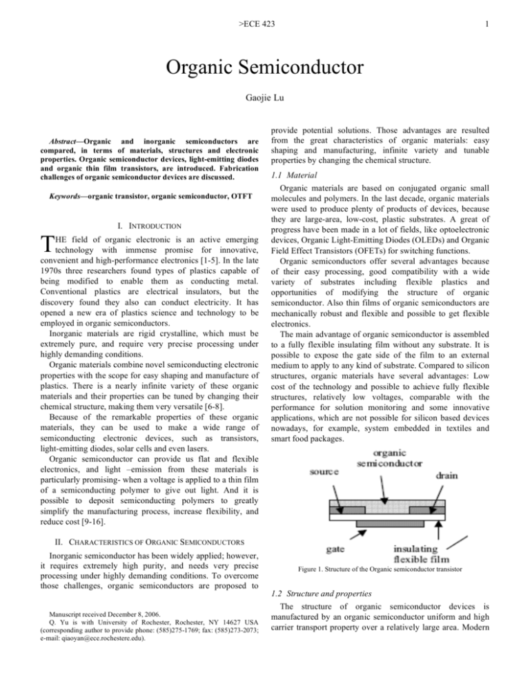
>ECE 423 1 Organic Semiconductor Gaojie Lu Abstract—Organic and inorganic semiconductors are compared, in terms of materials, structures and electronic properties. Organic semiconductor devices, light-emitting diodes and organic thin film transistors, are introduced. Fabrication challenges of organic semiconductor devices are discussed. Keywords—organic transistor, organic semiconductor, OTFT I. INTRODUCTION T HE field of organic electronic is an active emerging technology with immense promise for innovative, convenient and high-performance electronics [1-5]. In the late 1970s three researchers found types of plastics capable of being modified to enable them as conducting metal. Conventional plastics are electrical insulators, but the discovery found they also can conduct electricity. It has opened a new era of plastics science and technology to be employed in organic semiconductors. Inorganic materials are rigid crystalline, which must be extremely pure, and require very precise processing under highly demanding conditions. Organic materials combine novel semiconducting electronic properties with the scope for easy shaping and manufacture of plastics. There is a nearly infinite variety of these organic materials and their properties can be tuned by changing their chemical structure, making them very versatile [6-8]. Because of the remarkable properties of these organic materials, they can be used to make a wide range of semiconducting electronic devices, such as transistors, light-emitting diodes, solar cells and even lasers. Organic semiconductor can provide us flat and flexible electronics, and light –emission from these materials is particularly promising- when a voltage is applied to a thin film of a semiconducting polymer to give out light. And it is possible to deposit semiconducting polymers to greatly simplify the manufacturing process, increase flexibility, and reduce cost [9-16]. provide potential solutions. Those advantages are resulted from the great characteristics of organic materials: easy shaping and manufacturing, infinite variety and tunable properties by changing the chemical structure. 1.1 Material Organic materials are based on conjugated organic small molecules and polymers. In the last decade, organic materials were used to produce plenty of products of devices, because they are large-area, low-cost, plastic substrates. A great of progress have been made in a lot of fields, like optoelectronic devices, Organic Light-Emitting Diodes (OLEDs) and Organic Field Effect Transistors (OFETs) for switching functions. Organic semiconductors offer several advantages because of their easy processing, good compatibility with a wide variety of substrates including flexible plastics and opportunities of modifying the structure of organic semiconductor. Also thin films of organic semiconductors are mechanically robust and flexible and possible to get flexible electronics. The main advantage of organic semiconductor is assembled to a fully flexible insulating film without any substrate. It is possible to expose the gate side of the film to an external medium to apply to any kind of substrate. Compared to silicon structures, organic materials have several advantages: Low cost of the technology and possible to achieve fully flexible structures, relatively low voltages, comparable with the performance for solution monitoring and some innovative applications, which are not possible for silicon based devices nowadays, for example, system embedded in textiles and smart food packages. II. CHARACTERISTICS OF ORGANIC SEMICONDUCTORS Inorganic semiconductor has been widely applied; however, it requires extremely high purity, and needs very precise processing under highly demanding conditions. To overcome those challenges, organic semiconductors are proposed to Manuscript received December 8, 2006. Q. Yu is with University of Rochester, Rochester, NY 14627 USA (corresponding author to provide phone: (585)275-1769; fax: (585)273-2073; e-mail: qiaoyan@ece.rochestere.edu). Figure 1. Structure of the Organic semiconductor transistor 1.2 Structure and properties The structure of organic semiconductor devices is manufactured by an organic semiconductor uniform and high carrier transport property over a relatively large area. Modern >ECE 423 chemistry enables the synthesis of complex molecules, such as carbon, hydrogen, oxygen, and nitrogen atoms. They can be linked together with strong covalent bonds where two neighboring atoms each as addiction. F or non-covalent interactions, they can be built to complex supermolecular structures. They can approach nanotechnology; their interactions allow the materials to be tunable and mechanical properties. The structure of the Organic semiconductor transistor is shown in Figure 1. Carbon can form four bonds with neighboring carbon atoms or other atoms. Such as methane (CH4), four valence electrons occupy four sp3 in and can form four covalent bonds. When two adjacent carbon atoms come together, a band is formed between two electrons. We call it conjugated; atoms are linked by alternative double bonds. The contribution of change has been observed in the crystal structure with temperature to the variation of carrier mobility with temperature. With the temperature increasing, there will be slight increase in electron mobility along the crystal direction. Since the changes in crystal lattice dimensions of anthraquinone at various temperatures are small, the electronic band structure of organic compounds may be highly structure-sensitive. 2 (OLED) has been fabricated, which is made by pentacene films grown on flexible plastic structures [13]. A similar structure can be used also for detecting mechanical deformations on flexible surfaces, the flexibility of the substrate and the low cost of the employed technology, the production of flexible chemical and strain gauge sensors can be employed in a variety of innovative applications such as wearable electronics [14-16]. Over the last decade, blue Organic Light Emitting Diodes (blue OLEDs) with high efficiencies and advantages have attracted considerable attention for their potential applications to the full color ultra-thin flat panel display. Moreover, blue light can be converted into green or red with the use of proper dyes giving the possibility to generate all colors from the blue emitter. This latter property leads to an important simplification in the design of the OLEDs displays. Efficient blue OLEDs are doped transport layers in a p-i-n type structure. Figure 2 shows the molecular structure of the organic compounds used in this work, while Figure 3 details the layer structures of the two types of devices [15-17]. 1.3 Classification Organic semiconductors can be widely classified into two groups on the basis of their molecular weight: conjugated polycyclic compounds of molecular weight less than 1000, and heterocyclic polymers with molecular weight greater than 1000. Due to the ease with which they form thin films with large surface area, polymers are very useful materials for semiconductors. Small-molecule organic semiconductors may further be classified as linear, two-dimensional fused ring compounds, and heterocyclic oligomers. It is more facile control of charge transport by modifying various molecular parameters. Figure 2. Molecular Structures of the organic materials used for the Blue-Oled. III. ORGANIC SEMICONDUCTOR D EVICES 2.1 Organic Light-emitting diodes Light-emitting diode (LED) is a semiconductor device that light emits from a solid material, caused by an electrical power source. Its effect is a form of electroluminescence. The composition and condition of the semiconducting material used decide the color of the emitted light also can be infrared, such as visible or near-ultraviolet, infrared emission from gallium arsenide (GaAs) and other semiconductor alloys. A phenomenon termed electroluminescence is introduced here. The first light-emitting diode (LED) had been born. At that time, the properties of materials were poorly controlled, and the emission process was not well understood. The light-emitting active material was SiC crystallites, GaAs and AlGaAs as used for sandpaper abrasive. The first example of totally flexible field effect device for chemical detection based on an organic Light-emitting diode Figure 3. OLED structure with the detail of the thickness and the organic material used in each layers; (a) the emissive layer is DEC or PMC, (b) the emissive layer is DPVBi-doped with DEC or with PMC. 2.2 Organic thin film transistors Organic thin-film transistors (OTFTs) using organic semiconductor on organic semiconducting compounds in electronic components, notably computer displays, sensors, smart cards, and radio-frequency identification (RFID) tags. >ECE 423 Because OTFTs can be fabricated with a low-temperature process, they are more compatible with polymeric substrate than conventional silicon-based transistors. Organic thin-film transistors (OTFTs) inherit the design architecture from its inorganic counterpart MOSFET, and it consists of source, drain, and gate electrodes, a dielectric layer, and the active semiconductor layer, as shown in Figure.4 (a). As illustrated in Figure. 4 (b), the OTFT can achieve the typical I-V curves similar to that of MOSFET. The electrical characteristics of OTFTs were measured using two independent parameters: picoammeter/dc voltage sources. The OTFTs use a great deal of organic semiconductors in the field of lightweight, low-cost, large-area and flexible electronic products, and they become more compatible with polymeric substrate than conventional silicon-based transistors. Now it is successful to make it possible excellent electron mobility, such as n-type OTFT and excellent hole mobility [18]. There are ambipolar OTFTs and complementary inverters reported recently [19]. The performance of OTFTs has been steadily developed to fabricate those devices [20-21]. 3 extensively used in xerography. It can add certain combinations of amorphous organic semiconductors replaced amorphous Si and selenium as the active material in this application, which might be considered as the first large scale commercial application of an organic semiconductor. Small molecule and conjugated polymer light-emitting diodes are on the verge of commercialization. In order to improve the efficiency and stability of OTFTs devices, we have got impressive strides. Organic semiconductor based thin-film transistors have been proposed for number of applications, for example, displays and RFID tags, lower cost and simpler packaging with flexible substrates. They also appear in a wide range of photo-excited laser action, digital circuit, electronic noses, and so on. V. CONCLUSIONS Organic semiconductors pose a range of molecular weights and include small molecules. Because of chemical tenability, organic semiconductors become attractive materials for fabrication of FETs. Organic semiconductors remain the best performance, due to very well ordered structures. It has been proved that organic transistors fabrication is easier and cheaper than silicon transistors fabrication, although the carrier mobility is not sufficient fast. In addition, challenges exist in large-scale manufacturing. REFERENCES [1] [2] [3] [4] (a) [5] [6] [7] [8] [9] [10] [11] [12] [13] [14] [15] [16] [17] [18] [19] (b) [20] [21] [22] Figure. 4 Organic TFT (a) basic schematics [18] (b) I-V curves [19] IV. FUTURE WORK Organic semiconductors based photoconductors are H. E. Katz, Z. Bao, and S. J. Gilat, J. Acc. Chem. Res., vol.34, pp.359, 2001. Nandita Madhavan, “Small-molecule organic semiconductors,” April 01, 2002. A. Dodabalapur, “The future of organic semiconductor devices,” Device Research Conference 2000, Conference Digest, pp. 11-14, June 2000. http://assets.cambridge.org/052182/3307/excerpt/0521823307_excerpt.p df Shi J M and Tang C W, Appl. Phys. Lett. pp.80, 2002 http://www.aist.go.jp/aist_e/latest_research/2004/20041118/20041118.ht ml C. D. Dimitrakopoulos and D. J. Mascaro, “Organic thin-film transistors: A review of recent advances,” IBM J. Res. & Dev. Vol. 45, No. 1, Jan. 2001. http://www.drproctor.com/os/ www.st-andrews.ac.uk/~osc/org-semi.html C. Reese, M. Roberts, M. M. Ling and Z. Bao, “Organic thin film transistors,” materialstoday, pp.20-27, Sept. 2004. Gao Z Q, Lee C S, Bello I, Lee S T, Chen R M, Luh T Y, Shi J and Tang C W, Appl. Phys.Lett. pp.74, 1999 Kulkarni A P, Gifford A P, Tonzola C J and Jenekhea S A, Appl. Phys. Lett. pp.86, 2005 Gebeyehu D, et al., Synth. Met. Pp.148-205, 2005 Hosokawa C, Higashi H, Nakamura H and Kusumoto T, Appl. Phys. Lett. pp. 67, 1995 Liao C H, et al., Appl. Phys. Lett. pp. 86, 2005 Wu Y Z, et al. Appl. Phys.Lett. pp.83, 2003 Morin J F, Leclerc M, Adès D and Siove A, Macromol. Rapid Commun. pp. 761, 2005 http://www.oea-osc.com/persp_overview.htm http://www.phys.unsw.edu.au/~arh/background/Organic%20Electronics/ Organics.html A.Tsumura, H. Koezuka, and T. Ando, Appl.Phys.Lett. pp. 49, 1986 http://pubs.acs.org/hotartcl/ci/00/apr/0650wallace.html Y. Inoue, et al., “Organic Thin-file transistors with high electron mobility based on perfluoropentacene,” Japan Society of Applied Physics, Vol. 44, No. 6A pp. 3663-3668, 2005 >ECE 423 4
