HC55185 Ringing SLIC & AK2306/2306LV CODEC
Evaluation Board User Guide Supplement
TM
Application Note
January 2002
AN9992
Author: Don LaFontaine
Functional Description
This application note will first evaluate the DC performance
of the system by configuring the jumpers and hardware for
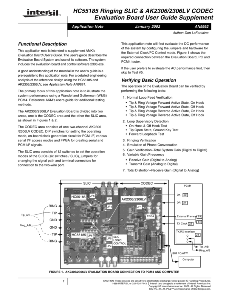
the External Clock/PC Control mode. Figure 1 shows the
required connection between the Evaluation Board, PC and
PCM4 tester.
This application note is intended to supplement AMK’s
Evaluation Board User’s Guide. The user’s guide describes the
Evaluation Board System and use of its software. The system
includes the evaluation board and control software 2306.exe.
If the user prefers to evaluate the AC performance first, then
skip to Test #5.
A good understanding of the material in the user’s guide is a
prerequisite to this application note. For a detailed engineering
analysis of the reference design using the HC55185 and
AK2306/2306LV, see Application Note AN9991.
Verifying Basic Operation
The operation of the Evaluation Board can be verified by
performing the following tests:
The primary focus of this application note is to illustrate the
system performance using a Wandel and Golterman (W&G)
PCM4. Reference AKM’s users guide for additional testing
methods.
1. Normal Loop Feed Verification
•
•
•
•
The AK2306/2306LV Evaluation Board is divided into two
areas, one is the CODEC area and the other the SLIC area,
as shown in Figures 1 & 2.
Tip &
Tip &
Tip &
Tip &
Ring Voltage Forward Active State, On Hook
Ring Voltage Forward Active State, Off Hook
Ring Voltage Reverse Active State, On Hook
Ring Voltage Reverse Active State, Off Hook
2. Loop Supervisory Detection
• On Hook & Off Hook Test
• Tip Open State, Ground Key Test
• Forward Loopback Test
The CODEC area consists of one two-channel AK2306
/2306LV CODEC, DIP switches for setting the operating
mode, on-board clock generation circuit for PCM I/F, various
serial I/F access modes and FPGA for creating serial and
PCM I/F signals.
3. Ringing Verification
4. Emulation of Phone Conversation
5. Gain Verification–Total System Gain (Digital to Digital)
6. Variable Gain/Frequency
The SLIC area consists of 12 switches to set the operation
modes of the SLICs (six switches / SLIC), jumpers for
changing the signal path and terminal connectors for
connection to the two-wire port.
• Receive Gain (Digital to Analog)
• Transmit Gain (Analog to Digital)
7. Total Distortion–Receive Gain (Digital to Analog)
SLIC
HC55185
JP6
JP5
RING
Tip_A/B
CODEC
AK2306/2306LV
JP4
PCM4
DX
20
DR
21
JP1
TIP
FPGA
External Frame
GND
Ring_A/B
TX Clock 22
63
61
GND
TIP
HC55185
RING
TX/RX Interface
JP6
JP5
JP4
24
SLIC
LOGIC
CONTROL
IBM PC/AT™
Tip_A/B
Ring_A/B
Computer
FIGURE 1. AK2306/2306LV EVALUATION BOARD CONNECTION TO PCM4 AND COMPUTER
1
CAUTION: These devices are sensitive to electrostatic discharge; follow proper IC Handling Procedures.
1-888-INTERSIL or 321-724-7143 | Intersil (and design) is a trademark of Intersil Americas Inc.
Copyright © Intersil Americas Inc. 2002. All Rights Reserved
IBM PC, XT, AT, PS/2™ are trademarks of IBM Corporation.
Application Note 9992
SLIC PART
J5
GND2
J6
VXMT_A
CODEC PART
VREC_A
VRS_A
GND2
VCCIO
VCCINT
GND1
Power
J1_A
JP6_A
JP1_A
J2_A
Channel
A
JP5_A
JP2_A
JP3_A
S2_A S3_A S4_A S5_A
S1_A
DR
TSYNC
RSYNC
JP4_A
SLIC
operation mode
S6_A
control SWJP7_A
J3_A
DX
LOOP
SLIC
J4_A
J15_A
BNC for PCM I/F
FS
FPGA
CODEC
J15_B
BCLK
J4_B
JP7_B
VBL
+5V
VREC_B
VCC
VXMIT_B
A
2
A
1
A
0
D
7
D
6
D
5
D
4
D
3
INT
BCLK_FRQ
ON
SYNC
JP3_B
VRS_B
VBH
SR_IF PCM_IF
JP4_B
SLIC
JP2_B
Terminal for 2-wire
analog port J1_B
FPGA control SW
JP5_B
JP1_B
J2_B
BNC for Analog I/F
S5_B S6_B
JP6_B
OFF
Channel
B
S2_B S3_B S4_B
EXT
J3_B S1_B
D
2
D
1
CN1
D
0
W
R
I
T
E
Serial I/F access SW
FIGURE 2. AK2306/2306LV MOTHER BOARD CONNECTIONS
HC55185 SLIC
The HC55185 is optimized to match a 600Ω line impedance,
have a ring trip threshold of 90mA, a switch hook threshold
of 12mA, loop current limit of 24.6mA and a transient current
limit of 100mA.
Programming of the logic state of the HC55185 is performed by
the toggle switches SW1 through SW6. Table 1 lists the switch
name (referenced to the SLIC data sheet), switch number
(reference to the PCB board layout), and the switch function.
The logic states of the HC55185 are shown in Table 2.
TABLE 1. TOGGLE SWITCHES FOR SLIC
SWITCH NAME SWITCH No.
FUNCTION
F2
S1
Logic control input
F1
S2
Logic control input
F0
S3
Logic control input
E0
S4
Selects between SHD,GKD and
RTD detectors (Table 2)
SWC
S5
Logic control for uncommitted
switch. Logic 0 switch on.
BSEL
S6
Selects either the high or low
battery supply for the HC55185
Logic 0 selects low battery
Logic 1 selects high battery
2
TABLE 2. HC55185 OPERATING MODES
MODE
F2
F1
F0
E0=1
E0=0
Low Power Standby
0
0
0
SHD
GKD
Forward Active
0
0
1
SHD
GKD
Unbalanced Ringing
0
1
0
RTD
RTD
Reverse Active
0
1
1
SHD
GKD
Ringing
1
0
0
RTD
RTD
Forward Loop Back
1
0
1
SHD
GKD
Tip Open
1
1
0
SHD
GKD
Power Denial
1
1
1
n/a
n/a
AK2306/2306LV Evaluation Board
The AK2306/2306LV Evaluation Board provides a way to
evaluate the operation of AKM’s CODEC and Intersil’s
HC55185 Ringing SLIC. Figure 2 shows the AK2306/2306LV
evaluation board component locations.
The programming interface illustrated in this application note
is once again the External Clock/PC Control mode. The
function of jumpers JP1_A/B through JP7_A/B are explained
in Table 3.
Application Note 9992
AK2306 (5V) Circuit Configuration:
TABLE 3. JUMPER CONNECTIONS
JUMPER
FUNCTION
1. Verify that resistor RIN_A/B is open (left of JP6_A/B).
2. Verify that capacitor CIN_A/B is open (left of JP6_A/B).
JP1_A/B
Connects uncommitted switch of HC55185 (SW-)
directly to the Ring terminal for loopback testing.
3. Jumper JP5_A/B has pin 3 shorted to pin 4.
JP2_A/B
Connects uncommitted switch of HC55185 (SW+)
through a 100Ω test load and diode to the Tip terminal
for loopback testing.
5. Verify RF_A/B is 120kΩ.
JP3_A/B
JP4_A/B
JP5_A/B
Connects the VBH supply terminal to the VBL supply
terminal for single supply applications.
4. Verify RA_A/B is 120kΩ.
6. Verify R8_A/B is 49.9kΩ.
AK2306LV (3.3V) Circuit Configuration:
1. Verify that resistor RIN_A/B is 45.3kΩ (left of JP6_A/B).
Short 1 to 2: Connects external VRS input to
HC55185 VRS input.
2. Verify that capacitor CIN_A/B is 0.47µF (left of JP6_A/B).
Short 3 to 4: Connects external VRS input through
TRAP (RC network) to HC55185 VRS input.
4. Verify RA_A/B is 42.2kΩ.
Short 5 to 6: Connects AK2306/2306LV ringing output
to the HC55185 VRS input.
6. Verify R8_A/B is 36.5kΩ.
3. Jumper JP5_A/B has pin 1shorted to pin 2.
5. Verify RF_A/B is 30.1kΩ.
Short 7 to 8: Connects the AK2306/2306LV receive
output to the HC55185 VRS input.
The following evaluation applies for both the AK2306 (5V) or
the AK2306LV (3.3V). Data presented was taken with the
AK2306 (5V) evaluation board.
Short 1 to 2: Shorts the receive input of the HC55185
to ground. AK2306LV operation only.
Configuring the board for operation:
Short 3 to 4: Connects receive output of
AK2306/2306LV to VRX input of HC55185.
JP6_A/B
Connects the HC55185 transmit output VTX to the
AK2306/2306LV amplifier for transhybrid balance.
JP7_A/B
Connects the GRS_0/1 output of the AK2306/2306LV
to the VFTN_0/1 input of the internal transhybrid
amplifier (AMPT).
Getting Started
TABLE 4. FPGA CONTROL SWITCHES
SWITCH
SW1
Selects PC mode
POSITION
O
SW3
Sets the SYNC timing
1
O
1
2
3
O
F
F
1
2
3
O
F
F
SW5
Selects normal operation, selects FS and BCLK
from external source (BNC)
O
F
F
SW4
Selects internal BCLK frequency(2.048M)
1
SW2
PCM I/F data format set to Long Frame (LF)
2
1
2
3
3
4. Configure SW1, SW2, SW3, SW4, SW5 as shown in
Table 4.
F
F
The evaluation board was built with either the AK2306 (5V)
CODEC or the AK2306LV (3.3V) CODEC (see Figure 1 for
placement of CODEC on the board). The following is a
check list to verify the correct components and jumper
placement for the CODEC on your board.
3. Connect the power supplies to the supply jacks on the
evaluation board.
2
The circuit schematics for the AK2306 and the AK2306LV
are different (reference Figures 7 and 8). The reason for the
different circuits is due to the low voltage (3.3V) operation of
the CODEC and the need to provide sufficient gain to the
two-wire loop. The smaller signal coming from the
AK2306LV (3.3V operation) needs to be gained up through
the SLIC, thus the variation in the two circuits.
2. Connect the PCM4 to the evaluation board as shown in
Figure 1.
F
F
The following steps will configure the Evaluation board for
testing the AK2306/2306LV and the HC55185 with the
PCM4. The operation mode selected to access the
AK2306/2306LV internal function registers are the External
Clock Mode (PCM interface operation) and the PC Control
Mode (Serial interface operation) using AKM proprietary
software. For other methods to control the PCM interface
and serial interface please reference AKM’s user’s guide.
1. Connect the IBM PC/AT (25 pin) cable between the
evaluation board and your computer (Figure 1).
Microsoft® Windows® 95 or higher should be installed
(Microsoft® Windows NT® is not supported).
Application Note 9992
7. Set the General Parameters of the PCM4 as shown in
Table 12 (see Test #5).
5. Verify JUMPER positions as shown in Table 5 or 6.
TABLE 5. AK2306 (5V) JUMPER CONNECTIONS
JUMPER
8. Initialize the software by clicking on file 2306.exe. The
internal register data of AK2306/2306LV will be initialized
and the Register Map will be displayed (reference Table
8). Table 10 lists the Register functions in more detail.
FUNCTION
JP1 (CODEC side)
open
JP4 (CODEC side)
Short pin 1 to pin 2
JP4_A/B
Short pin 5 to pin 6
JP5_A/B
Short pin 3 to pin 4
JP6_A/B
Short pin 1 to pin 2
All Other Jumpers
Open
9. On the computer terminal, entering a “1” will enable the
user to program the AK2306/2306LVs: Receive and
Transmit gains, exercise the CODECs power down
controls, mute control, PCM interface select, PCM data
channel select, A/µ-law select and Tone frequency select
(reference Table 10).
10. Input the register address (column 1 of Table 10) in
decimal form (0–7) for the function you wish to program.
For example, if you wanted to change the receive gain for
channel 0 you would type in ‘0’ and press return.
TABLE 6. AK2306LV (3.3V) JUMPER CONNECTIONS
JUMPER
FUNCTION
NOTE: the default receive gain is 0dB.
JP1 (CODEC side)
Open
JP4 (CODEC side)
Open
JP4_A/B
Short pin 5 to pin 6
JP5_A/B
Short pin 1 to pin 2
JP6_A/B
Short pin 1 to pin 2
All Other Jumpers
Open
6. Configure the HC55185 to be in the Forward Active mode
using the SLIC Operation Mode Control Switches
S1_A/B through S6_A/B. Reference Table 7 for switch
positions. (Note: Switch position for logic 1 is towards the
top of the board and logic 0 towards the bottom.)
11. To change the default values of any of the CODEC’s
functions (Table 10), the user must input the
corresponding number in a two-digit hexadecimal
number. Table 9 can be used as a quick reference guide
for programming the gains through the CODEC using
hexadecimal numbers. Row one lists the available
programming gains in dB, row two lists the corresponding
two-digit hexadecimal number for that gain and row three
lists the binary number that will appear on the computer
screen after the user inputs the two-digit hexadecimal
number.
12. The SLIC is now ready to be tested.
TABLE 7. PROGRAMING HC55185 OPERATING MODES
HC55185
MODE
S1
(F2)
S2
(F1)
S3
(F0)
S4
(E0)
S5
(SWC)
S6
(BSEL)
Low Power Standby
0
0
0
1
--
0
Forward Active
0
0
1
1
--
0
Unbalanced Ringing
0
1
0
1
--
1
Reverse Active
0
1
1
1
--
0
Ringing
1
0
0
1
--
1
Forward Loopback
1
0
1
1
--
0
Tip Open
1
1
0
1
--
0
Power Denial
1
1
1
1
--
0
4
Microsoft®, Windows® and Windows NT® are registered trademarks of Microsoft Corporation
Application Note 9992
TABLE 8. REGISTER MAP
A2
A1
A0
D7
D6
D5
D4
D3
D2
D1
D0
0
0
0
TST13
TST12
-
GA0R4
GA0R3
GA0R2
GA0R1
GA0R0
0
0
1
TST11
TST10
-
GA1R4
GA1R3
GA1R2
GA1R1
GA1R0
0
1
0
TST9
TST8
-
GA0T4
GA0T3
GA0T2
GA0T1
GA0T0
0
1
1
TST7
TST6
-
GA1T4
GA1T3
GA1T2
GA1T1
GA1T0
1
0
0
TST5
TST4
MTCH1
MTCH0
PD
PDTN
PDCH1
PDCH0
1
0
1
TST3
TST2
TST1
TST0
TNFQ
ALAWN
SEL2B
PCMIF
1
1
0
Reserved
1
1
1
Reserved
TABLE 9. RERERENCE GUIDE TO CONVERT GAIN TO CORRESPONDING HEXADECIMAL NUMBER
Gain (dB)
6
5
4
3
2
1
0
-1
-2
-3
-4
-5
-6
-7
-8
-9
-10
-11
-12
-13
-14
-15
-16
-17
-18
Hex #
0
1
2
3
4
5
6
7
8
9
A
B
C
D
E
F
10
11
12
13
14
15
16
17
18
Binary #
0
0
0
0
0
1
0
0
0
0
0
1
0
0
0
1
1
0
0
0
0
0
1
0
0
1
0
1
0
0
0
1
1
0
0
1
1
1
0
0
0
0
0
1
0
1
0
0
1
0
0
1
0
1
0
1
1
0
1
0
0
0
1
1
0
1
0
1
1
0
0
1
1
1
0
1
1
1
1
0
0
0
0
0
1
1
0
0
0
1
0
1
0
0
1
1
1
0
0
1
0
0
1
0
1
1
0
1
0
1
0
1
1
0
1
1
1
1
0
1
0
0
0
1
1
TABLE 10. REGISTER FUNCTIONS
Address
Bit
Name
Default
000
0
GA0R0
0
1
GA0R1
1
2
GA0R2
1
3
GA0R3
0
4
GA0R4
0
5
-
6
0
0
7
0
0
0
GA1R0
0
1
GA1R1
1
2
GA1R2
1
3
GA1R3
0
4
GA0R4
0
5
-
6
0
0
7
0
0
001
5
Function
Receive gain adjustment on ch0
+6 to –18dB in 1dB steps
00000: +6dB 11xxx: -18dB
Test mode
Please write all “0”.
Receive gain adjustment on ch1
+6 to –18dB in 1dB steps
00000: +6dB 11xxx: -18dB
Test mode
Please write all “0”.
Application Note 9992
TABLE 10. REGISTER FUNCTIONS (Continued)
Address
Bit
Name
Default
010
0
GA0T0
0
1
GA0T1
1
2
GA0T2
1
3
GA0T3
0
4
GA0T4
0
5
-
6
0
0
7
0
0
0
GA1T0
0
1
GA1T1
1
2
GA1T2
1
3
GA1T3
0
4
GA1T4
0
5
-
6
0
0
7
0
0
0
PDCH0
0
1
PDCH1
0
2
PDTN
1
RING TONEGEN Power down control
0: Power ON 1: Power OFF
3
PD
0
Full Power down
0: Power ON 1: Power OFF
4
MTDX0
0
5
MTDX1
0
Mute control: VR0.VR1,DX pin
0: Normal output 1: Mute
6
0
0
7
0
0
0
PCMIF
0
PCM Interface select
0: LF/SF 1: GCI
1
SEL2B
0
PCM data channel select
0: CH0ÆB1 1: CH1ÆB1
2
ALAWN
1
A/µ-law select
0: A-law 1: µ-law
3
TNFQ
0
Tone frequency select
0: 16Hz 1: 20Hz
4
0
0
5
0
0
Test mode
Please write all “0”.
6
0
0
7
0
0
011
100
101
Function
Transmit gain adjustment on ch0
+6 to -18dB in 1dB steps
00000: +6dB 11xxx: -18dB
Test mode
Please write all “0”.
Transmit gain adjustment on ch1
+6 to -18dB in 1dB steps
00000: +6dB 11xxx: -18dB
Test mode
Please write all “0”.
CODEC CH0,1 Power down control
0: Power ON 1: Power OFF
Test mode
Please write all “0”.
110
Reserved
111
Reserved
6
Application Note 9992
Test # 1 Normal Loop Feed Verification
This test verifies the correct tip and ring voltages in both
onhook and offhook forward active and reverse active
states. Loop current and ground key are also verified via
on-board LEDs.
When the forward loop back mode is initiated internal
switches connect a 600Ω load across the outputs of the Tip
and Ring amplifiers as shown in Figure 4.
TIP
TIP AMP
Discussion
The HC55185 is designed to have its most positive two-wire
terminal (tip in the forward active state and ring in the
reverse active state) fixed at a set voltage. The most
negative two-wire terminal voltage is dependent upon the
load across tip and ring and the programmable current limit.
Loop supervision is provided by either the switch hook or the
ground key detectors. Loop status is observed by monitoring
CR2_A/B LED on the board. The device may be operated from
either high or low battery for on-hook transmission, during
ringing and low battery for loop feed.
When operating from the high battery, the DC voltages at Tip
and Ring are MTU compliant. The typical Tip voltage is -4V
and the Ring voltage is a function of the battery voltage for
battery voltages less than -60V as shown in Equation 1.
(EQ. 1)
V RING = V BH + 4
Most applications will operate the device from low battery
while off hook. The DC feed characteristic of the device will
drive Tip and Ring towards half battery to regulate the DC
loop current. For light loads, Tip will be near -4V and Ring
will be near VVBL + 4V. Figure 3 shows the DC feed
characteristic.
VTR(OC)
VTR , DC (V)
m = (∆VTR /∆IL) = 11.1kΩ
ILOOP (mA)
RING
RING AMP
FIGURE 4. FORWARD LOOP BACK INTERNAL TERMINATION
When the internal signal path is provided, DC current will
flow from Tip to Ring. The DC current will force DET low
causing current to flow through CR2_A/B, turning on the
diode.
Measuring Tip and Ring Voltages
1. Configure Hardware and Software as described in section
titled Getting Started.
2. Configure the HC55185 to be in the forward active mode
using the SLIC operation mode control switches S1_A/B
through S6_A/B. Reference Table 7 for switch positions.
(Note: Switch position for logic 1 is towards the top of the
board and logic 0 towards the bottom.)
3. Measure the tip and ring voltages (reference Figure 1)
and compare to those in Table 11 (onhook).
4. Terminate TIP and RING with a 600Ω load via the banana
jacks or the RJ11 jack.
5. Measure tip and ring voltages with respect to ground and
compare to those in Table 11 (offhook 600Ω).
7. Disconnect the 600Ω load from across tip and ring.
FIGURE 3. DC FEED CHARACTERISTIC
8. Repeat steps 3, 4 and 5.
The point on the y-axis labeled VTR(OC) is the open circuit
Tip to Ring voltage and is defined by the feed battery
voltage.
(EQ. 2)
The Ground Key detector operation is verified by configuring
the HC55185 in the tip open state and grounding the ring
pin. Grounding the ring pin results in a current that triggers
an internal detector that pulls the output of DET low causing
current to flow through CR2_A/B, turning on the diode.
The Forward Loop Back mode provides test capability for the
device. An internal signal path is enabled allowing for both
DC and AC verification. The internal 600Ω terminating
resistor has a tolerance of ±20%. The HC55185 is intended
to operate from only the low battery during this mode.
7
HC55185
6. Configure the HC55185 to be in the Reverse Active mode
using the SLIC Operation Mode Control Switches
S1_A/B through S6_A/B. Reference Table 7 for switch
positions.
ILIM
V TR ( OC ) = VBL – 8
600Ω
TABLE 11. TIP AND RING VOLTAGES
RL
(Ω )
TIP VOLTAGE
REFERENCED
TO GND
RING VOLTAGE
REFERENCED
TO GND
Forward Active
VBH = -48V
V BL = NA
VCC = +5V
Onhook
-3.6 to -4.6
-17.2 to -21.1.0
Offhook
600Ω
-4.6 to -5.6
-16.2 to -19.7
Reverse Active
VBH = -48V
V BL = NA
VCC = +5V
Onhook
-17.2 to -21.1.0
-3.6 to -4.6
Offhook
600Ω
-16.2 to -19.7
-4.6 to -5.6
LOGIC STATE
Application Note 9992
Test # 2 Loop Supervisory Detection
Verification of Switch Hook Detect
If previous test was Test #1, skip to step 3.
1. Configure Hardware and Software as described in section
titled Getting Started.
2. Configure the HC55185 to be in the forward active mode
using the SLIC operation mode control switches S1_A/B
through S6_A/B. Reference Table 7 for switch positions.
3. With the SLIC in either the forward active state (Active F)
or reverse active state (Active R), the LED CR2_A/B is on
when tip and ring are terminated with 600Ω and off when
tip and ring are an open circuit.
4. Disconnect the 600Ω load from across tip and ring.
Verification of Ground Key Detect
1. Configure the HC55185 to be in the Tip Open mode using
the SLIC operation mode control switches S1_A/B
through S6_A/B. Reference Table 7 for switch positions.
2. Grounding the ring terminal will verify ground key detect
when the CR2_A/B diode turns on.
Verification of Forward Loopback
1. Configure the HC55185 to be in the forward loop back
mode using the SLIC operation mode control switches
S1_A/B through S6_A/B. Reference Table 7 for switch
positions.
2. Verification of forward loopback operation is when both
the CR2_A/B (SHD) and CR1_A/B (ALM) diodes turn on.
Test # 3 Ringing Verification
This test will demonstrate the ability of the AK2306/2306LV
to ring a phone through the HC55185. A telephone is the
only additional hardware required to complete this test.
Discussion
The HC55185 provides linear amplification to support a
variety of ringing waveforms. A programmable ring trip
function provides loop supervision and auto disconnect upon
ring trip. The device is designed to operate from the high
battery during this mode.
Architecture
The device provides linear amplification to the signal applied
to the ringing input, VRS . The differential ringing gain of the
device is 80V/V. The circuit model for the ringing path is
shown in Figure 5.
The voltage gain from the VRS input to the Tip output is
40V/V. The resistor ratio provides a gain of eight and the
current mirror provides a gain of five. The voltage gain from
the VRS input to the Ring output is -40V/V. The equations for
the Tip and Ring outputs during ringing are given in
Equations 3 and 4.
V BH
V T = ----------- + ( 40 × VRS )
2
(EQ. 3)
VBH
V R = ----------- – ( 40 × VRS )
2
(EQ. 4)
R
TIP
20
R/8
+
5:1
RING
-
+
-
20
+
-
VRS
600K
+ VBH
2
R
FIGURE 5. LINEAR RINGING MODEL
When the input signal at VRS is zero, the Tip and Ring
amplifier outputs are centered at half battery. The device
provides auto centering for easy implementation of
sinusoidal ringing waveforms. Both AC and DC control of the
Tip and Ring outputs are available during ringing. This
feature allows for DC offsets as part of the ringing waveform.
Ringing Input
The ringing input, VRS , is a high impedance input. The high
impedance allows the use of low value capacitors for AC
coupling the ring signal. The VRS input is enabled only
during the ringing mode, therefore a free running oscillator
may be connected to VRS at all times.
When operating from a battery of -100V, each amplifier, Tip
and Ring, will swing a maximum of 95VP-P . Hence, the
maximum signal swing at VRS to achieve full scale ringing is
approximately 2.4VP-P . The low signal levels are compatible
with the output voltage range of the CODEC. The digital
nature of the CODEC ideally suits it for the function of
programmable ringing generator.
Ringing the Phone
If previous test was either Test #1 or #2, skip to Step 2.
1. Configure hardware and software as described in section
titled Getting Started.
2. Configure the HC55185 to be in the Ringing mode using
the SLIC Operation Mode Control Switches S1_A/B
through S6_A/B. Reference Table 7 for switch positions.
Keep BSEL LOW at this point.
3. Press ‘1’ to write to the CODEC resisters. Then decimal 4
followed by Hex 00. This will power up the ring tone
generator.
4. Press ‘1’ to write to the CODEC resisters. Then decimal 5
followed by Hex 06. This will set the ring tone generator
to 20Hz.
5. Connect a phone to Channel A/B using the RJ11 jack on
the board.
6. Toggle the BSEL switch S6_A/B from low battery to high
battery and the phone will start to ring.
8
Application Note 9992
7. When the test is completed, set the BSEL switch S6_A/B
low. You also need to power down the ring generator.
Press ‘1’ to write to the CODEC resisters. Then decimal
4 followed by Hex 04.This will prevent the tone from
interfering with subsequent tests.
SW5
F
F
O
1
2
3
4. Connect the DX terminal (connected to port 20 of PCM4)
to the DR terminal (connected to port 21 of PCM4).
8. Configure the HC55185 to be in the forward active mode
using the SLIC operation mode control switches S1_A/B
through S6_A/B. Reference Table 7 for switch positions.
5. Verify that the Ring tone generator is turned off. Press ‘1’
to write to the CODEC resisters. Then decimal 4 followed
by Hex 04.
Test # 4 Emulation of Phone Conversation
Verification of Phone Conversation
This test will demonstrate an end to end phone conversation
between Channel A and Channel B. Setting up an end to
end phone conversation is accomplished configuring the
AK2306/2306LV for the swap mode and connecting the DX
and DR terminals together (Figure 1).
1. Verify phone connection between both channels by
picking up the receivers and talking.
2. Return dip switch SW5 to initial position (Table 4).
3. Reconnect DX and RX to PCM4.
If previous test was either Test #1, #2 or #3, skip to step 3.
Test # 5 Gain Verification
1. Configure hardware and software as described in section
titled Getting Started.
This test will verify the gains through the AK2306/2306LV
and the HC55185 are operating properly. The test will show,
with the receive and transmit gains programmed to 0dB, the
Digital to Analog gain across both the CODEC and the SLIC
is equal to -1.0 (0dB), and the Analog to Digital gain across
both the SLIC and the CODEC is also equal to 1.0 (0dB).
Both D/A and A/D gains will be verified by performing a
Digital to Digital gain using the PCM4.
2. Configure both HC55185s in the forward active mode
using the SLIC operation mode control switches S1_A/B
through S6_A/B. Reference Table 7 for switch positions.
3. Configure DIP switch SW5 for the swap mode by toggling
2 in the off position as shown.
G4-2
R7
33K
0.7745VRMS
INTERSIL
HC55185 (1 OF 8)
RP
49Ω
TIP
+
V2W
-
R6
33K
VRX
CRX
0.47µF
+
ZL
VTR
-
EG
ZTR
VFR
GSR
CA
0.47µF
RF
ZO
R8
49.9K
VTX
ZO = ZL - 2RP
120K
CTX
0.47µF
RS
66.5K
AMPR AMPLIFIER
PCM
BUS
GST
AMPT AMPLIFIER
VFTN
VFTP
-IN
0dBm0(600Ω)
CFB
0.7745VRMS
0.7745VRMS
DR
RECIEVE PATH
GAIN
0dB
RA
120K
RING
RP
49Ω
0dBm0 (600Ω)
AK2306
VRO
0dBm0(600Ω)
+
-
0.7745VRMS
SYSTEM REQUIREMENTS:
IMPEDANCE: 600Ω
TRANSMIT GAIN (A/D): +5.0dB
RECEIVE GAIN (D/A): 0dB
+
-
0dBm0(600Ω)
VFB
4.7µF
TRANSMIT PATH
GAIN
0dB
-7.619dBm0(600Ω)
0dBm0(600Ω)
0dBm0(600Ω)
0.32219VRMS
0.7748VRMS
0.7748VRMS
G2-4
FIGURE 6. REFERENCE DESIGN OF THE HC55185 AND THE AK2306 WITH A 600Ω LOAD IMPEDANCE
Figure 6 shows the reference design of the HC55185 and
the AK2306 with a 600Ω load impedance. Reference
Application Note AN9991 for a detailed engineering analysis
of the reference design.
9
DX
Application Note 9992
Total System Gain (D/D)
If previous test was Test #1, #2, #3, or #4, skip to Step 3.
1. Configure hardware and software as described in section
titled Getting Started.
2. Configure the HC55185 to be in the forward active mode
using the SLIC operation mode control switches S1_A/B
through S6_A/B. Reference Table 7 for switch positions.
TABLE 12. PCM4 GENERAL PARAMETERS
SETTINGS (Continued)
General Parameter
(9) Special Parameter:
Level Display
Two wire Term.
Digital Channel no.
Setting
dBm0
Infinite
Time Slot
Mark and cont.
Tolerance mask set 2
3. Terminate tip and ring with a 600Ω load.
4. Set the general parameters of the PCM4 as shown in
Table 12. Set the PCM4 Interface (port 14) to TX/RX. Set
the RX-Impedance/Ω (port 13) to 600Ω. Set the
TX-Impedance/Ω (port 15) to 600Ω.
Clock display
OFF
Mark and cont.
OFF
Parm
11
13
16
22
23
27
33
35
5. Set the PCM4 transmit and receive channels to
channel 0. This will enable the PCM4 to receive and
transmit data to the Channel A PCM time slot. To test
channel B, set the PCM4 to channel 1.
6. Configure the PCM4 for the MODE A 11 test. Set PCM4
to D-D, SWP/S (single sweep). Press start to test
network.
Verification
Compare results to the Graph 1.
TABLE 12. PCM4 GENERAL PARAMETERS
SETTINGS
General Parameter
Setting
(1) Digital Configuration:
General configuration
Parm
TX/RX 2M/2Mbps
selected
OPEN/AUX.SIGN.
11
(2) Frame Selection:
TX frame type
RX frame type
CRC-4 Multiframe
All 32 TS teleph
All 32 TS teleph
Off
14
24
31
(3) Digital TX Interface:
Line Code
Output Impedance
Clock
NRZ
75Ω unbalanced
Int. 2048kHz
13
22
31
(4) Digital RX I nterface:
Line Code
Input Impedance
NRZ
> 3kΩ
13
22
Reset to standard values
ALL CHAN.
11
22
Off
11
Variable Gain / Frequency (D/A) Test #6a
Must match address 101
Table 10. Default
setting is µ-law
11
If previous test was Test #1, #2, #3, or #4, skip to Step 3. If
previous test was Test # 5 skip to Step 5.
RX Encoding Law
Must match encoding law
21
(8) Scanner Parameter:
VF-Input no.
VF-Output no.
1
1
11
21
Digital Loop (A - A)
(5) Digital Words in TX
Frame:
Frame Words
Send Signal
(6) TX Error Insertion
(7) PCM Coding:
TX Encoding Law
10
23
GRAPH 1. TOTAL SYSTEM GAIN (D/D)
Test # 6 Variable Gain / Frequency
This test will configure the HC55185 in the loopback mode
and evaluate the AK2306/2306LV and the HC55185’s AC
performance across frequency.
Discussion
Most of the SLICs in the HC55185 family feature two-wire
loopback testing. During the two-wire loopback test, a 600Ω
internal resistor is switched across the tip and ring terminals
of the SLIC. This allows the DET function and the four-wire
to four-wire AC transmission, right up to the subscriber loop,
to be tested.
1. Configure hardware and software as described in section
titled Getting Started.
2. Configure the HC55185 to be in the forward loop back
mode using the SLIC operation mode control switches
S1_A/B through S6_A/B. Reference Table 7 for switch
positions.
Application Note 9992
3. Set the general parameters of the PCM4 as shown in
Table 12. Set the PCM4 Interface (port 14) to TX/RX. Set
the RX-Impedance/Ω (port 13) to 600Ω. Set the
TX-Impedance/Ω (port 15) to 600Ω.
4. Set the PCM4 transmit and receive channels to
channel 0. This will enable the PCM4 to receive and
transmit data to the Channel A PCM time slot. To test
channel B, set the PCM4 to channel 1.
5. Remove the 600Ω load from across tip and ring.
6. Configure the PCM4 for the MODE A 33 test. Set PCM4
to D-A, SWP/S (single sweep). Press start to test
network.
Verification
Compare results to the Graph 2.
Test # 7 Total Distortion
This test will configure the HC55185 in the loopback mode
and evaluate the AK2306/2306LV and the HC55185’s total
distortion.
Total Distortion (D/A) Test #7
If previous test was Test # 1, #2, #3, or #4, skip to Step 3.
If previous test was Test # 5 skip to Step 4.
If previous test was Test #76a/b skip to Step 6.
1. Configure hardware and software as described in section
titled Getting Started
2. Set the general parameters of the PCM4 as shown in
Table 12. Set the PCM4 Interface (port 14) to TX/RX. Set
the RX-Impedance/Ω (port 13) to 600Ω. Set the
TX-Impedance/Ω (port 15) to 600Ω.
3. Set the PCM4 transmit and receive channels to
channel 0. This will enable the PCM4 to receive and
transmit data to the Channel A PCM time slot. To test
channel B, set the PCM4 to channel 1.
4. Configure the HC55185 to be in the forward loop back
mode using the SLIC operation mode control switches
S1_A/B through S6_A/B. Reference Table 7 for switch
positions.
5. Remove the 600Ω load from across tip and ring.
6. Configure the PCM4 for the MODE A 55 test. Set PCM4
to D-A, SWP/S (single sweep). Press start to test
network.
Verification
Compare results to the Graph 4.
GRAPH 2. (D/A) VARIABLE GAIN vs. FREQUENCY
Variable Gain / Frequency (A/D) Test #6b
1. Configure the PCM4 for the MODE A 33 test. Set PCM4
to A-D, SWP/S (single sweep). Press start to test
network.
Verification
Compare results to the Graph 3.
FIGURE 4. (D/A) TOTAL DISTORTION
GRAPH 3. (A/D) VARIABLE GAIN vs. FREQUENCY
11
Application Note 9992
Board Schematic
R
I
+ M
-
V2
20Ω
RP
IM
-
IX RECEIVE BLOCK
V1
+
R7
33K
IX
VIN
1:1
FEED
AMPLIFIER
R
VTR
+
VRX
RING
FEED
AMPLIFIER
RSENSE
V3
V4
+
20Ω
IX
- IM +
+
R
TA
FEEDBACK AMPLIFIER
3R
4R
4R
+
4R
3R
R8
49.9K
+ CTX
VTX 0.47µF
-
+
4R
VTX
8K
GSR
RA
120K
AMPR
AMPLIFIER
PCM I/F
120K
VFTN
VFTP
RS
66.5K
-IN
CFB
VFB
VSA = ∆IM30
SENSE AMPLIFIER
FS
BCLK
GST
FIGURE 7. HC55185 SIMPLIFIED AC TRANSMISSION CIRCUIT AND AK2306
12
DR
VFR
CA
0.47µF
RF
E
- G
RP
RECEIVE PATH
R
+
- IM +
R6
33K
+ CRX
VRX 0.47µF
-
Z0
+
+
V2W
-
I
+ M
ZL
-
RSENSE
AK2306
VRO
+
-
TIP
INTERSIL
+ HC55185 (1 OF 2)
+
-
IX
-
AMPT
AMPLIFIER
TRANSMIT PATH
DX
Application Note 9992
Board Schematic (continued)
R
I
+ M
-
V2
20Ω
RP
IM
-
IX RECEIVE BLOCK
V1
+
R7
33K
IX
VIN
1:1
FEED
AMPLIFIER
R
VTR
+
VRX
RP
GSR
CA
0.47µF
RA
42.2K
RF
E
- G
RING
RECEIVE PATH
0dB
FEED
AMPLIFIER
RSENSE
V3
V4
+
20Ω
IX
- IM +
+
R
VTX
PCM I/F
4R
+
4R
4R
3R
+
3R
VFTP
8K
RS
66.5K
-IN
AMPT
AMPLIFIER
TRANSMIT PATH
0dB
DX
RIN
45.3K
CFB CIN
VFB 0.47µF
VSA = ∆IM30
FS
BCLK
GST
30.1K
VFTN
+ CTX
VTX 0.47µF
-
TA
FEEDBACK AMPLIFIER
4R
R8
36.5K
DR
AMPR
AMPLIFIER
R
+
- IM +
VFR
R6
33K
+ CRX
VRX 0.47µF
-
Z0
+
+
V2W
-
I
+ M
ZL
-
RSENSE
AK2306LV
VRO
+
-
TIP
INTERSIL
+ HC55185 (1 OF 2)
+
-
IX
-
RECEIVE GAIN FROM DR TO T/R IS +3.3dB
TRANSMIT GAIN FROM T/R TO DX IS -9.3dB
SENSE AMPLIFIER
AK2306LV
LOW VOLTAGE CONNECTION
FIGURE 8. HC55185 DEMO DAUGHTER BOARD SCHEMATIC
All Intersil U.S. products are manufactured, assembled and tested utilizing ISO9000 quality systems.
Intersil Corporation’s quality certifications can be viewed at www.intersil.com/design/quality
Intersil products are sold by description only. Intersil Corporation reserves the right to make changes in circuit design, software and/or specifications at any time without
notice. Accordingly, the reader is cautioned to verify that data sheets are current before placing orders. Information furnished by Intersil is believed to be accurate and
reliable. However, no responsibility is assumed by Intersil or its subsidiaries for its use; nor for any infringements of patents or other rights of third parties which may result
from its use. No license is granted by implication or otherwise under any patent or patent rights of Intersil or its subsidiaries.
For information regarding Intersil Corporation and its products, see www.intersil.com
Sales Office Headquarters
NORTH AMERICA
Intersil Corporation
7585 Irvine Center Drive
Suite 100
Irvine, CA 92618
TEL: (949) 341-7000
FAX: (949) 341-7123
Intersil Corporation
2401 Palm Bay Rd.
Palm Bay, FL 32905
TEL: (321) 724-7000
FAX: (321) 724-7946
13
EUROPE
Intersil Europe Sarl
Ave. William Graisse, 3
1006 Lausanne
Switzerland
TEL: +41 21 6140560
FAX: +41 21 6140579
ASIA
Intersil Corporation
Unit 1804 18/F Guangdong Water Building
83 Austin Road
TST, Kowloon Hong Kong
TEL: +852 2723 6339
FAX: +852 2730 1433
