Test 2 Version B Solutions
advertisement
1
ECE371
Test 2
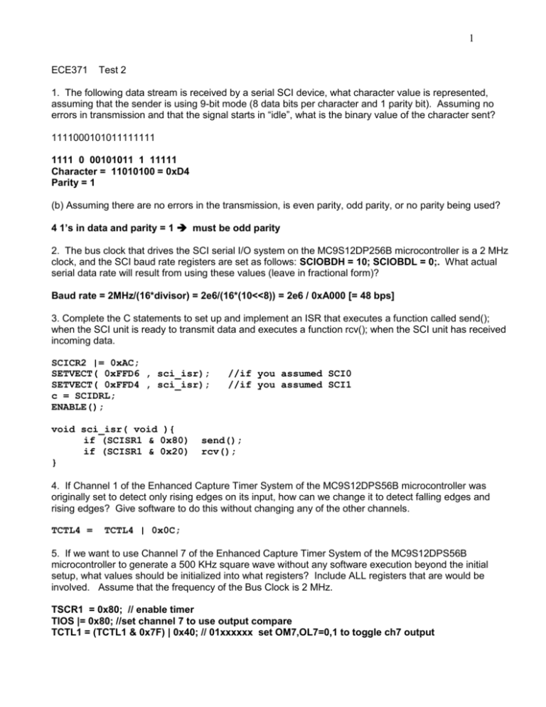
1. The following data stream is received by a serial SCI device, what character value is represented,
assuming that the sender is using 9-bit mode (8 data bits per character and 1 parity bit). Assuming no
errors in transmission and that the signal starts in “idle”, what is the binary value of the character sent?
1111000101011111111
1111 0 00101011 1 11111
Character = 11010100 = 0xD4
Parity = 1
(b) Assuming there are no errors in the transmission, is even parity, odd parity, or no parity being used?
4 1’s in data and parity = 1 must be odd parity
2. The bus clock that drives the SCI serial I/O system on the MC9S12DP256B microcontroller is a 2 MHz
clock, and the SCI baud rate registers are set as follows: SCIOBDH = 10; SCIOBDL = 0;. What actual
serial data rate will result from using these values (leave in fractional form)?
Baud rate = 2MHz/(16*divisor) = 2e6/(16*(10<<8)) = 2e6 / 0xA000 [= 48 bps]
3. Complete the C statements to set up and implement an ISR that executes a function called send();
when the SCI unit is ready to transmit data and executes a function rcv(); when the SCI unit has received
incoming data.
SCICR2 |= 0xAC;
SETVECT( 0xFFD6 , sci_isr);
SETVECT( 0xFFD4 , sci_isr);
c = SCIDRL;
ENABLE();
void sci_isr( void ){
if (SCISR1 & 0x80)
if (SCISR1 & 0x20)
}
//if you assumed SCI0
//if you assumed SCI1
send();
rcv();
4. If Channel 1 of the Enhanced Capture Timer System of the MC9S12DPS56B microcontroller was
originally set to detect only rising edges on its input, how can we change it to detect falling edges and
rising edges? Give software to do this without changing any of the other channels.
TCTL4 =
TCTL4 | 0x0C;
5. If we want to use Channel 7 of the Enhanced Capture Timer System of the MC9S12DPS56B
microcontroller to generate a 500 KHz square wave without any software execution beyond the initial
setup, what values should be initialized into what registers? Include ALL registers that are would be
involved. Assume that the frequency of the Bus Clock is 2 MHz.
TSCR1 = 0x80; // enable timer
TIOS |= 0x80; //set channel 7 to use output compare
TCTL1 = (TCTL1 & 0x7F) | 0x40; // 01xxxxxx set OM7,OL7=0,1 to toggle ch7 output
2
TIE &= 0x7F; //0xxxxxxx, disable channel 7 timer interrupt
TSCR2 = 0x09; // 00001001 set TCRE and set prescale to 1
TC7 = 1; // with prescale = 1, toggle output every count (T/2 = 1 µs)
6. Assume that Channel 0 of the Enhanced Capture Timer System of the MC9S12DPS56B
microcontroller is being used to measure the width on an incoming pulse. What is the pulse width in
milliseconds if the following conditions are present (can be left as a mathematical expression)?
• The input clock to the Timer/Control Unit has a frequency of 2 MHz
• Timer System Control Register 2 was initialized to 00000010
• When a rising edge is detected, a value of 1000 hex is read from register TC0.
• When the next falling edge is detected after one TCNT overflow event, a value of 3000 hex is detected.
Prescale is 2, divider is 4, each count is 2 µs
0x3000-0x1000+0x10000 = 0x12000
0x12000 * 2 µs = 0x24000 µs [= 147.5 ms]
7. What effect does the following software have on the MC9S12DPS56B microcontroller's Timer/Counter
unit:
TIOS = 0x42;
01000010 channels 6 and 1 are outputs, channels 0, 2-5, and 7 are inputs
TCTL3 = 0x27
00 10 01 11 channel 7 is disabled, channel 6—no effect, output, channel 5 will capture the
time of rising edges, channel 4 will capture the time of rising and falling edges
8. Give the values of the OC7M and OC7D register for the Enhanced Counter/Timer Unit of the
MC9S12DP256B microcontroller so that when Channel 7's register value is the same as the current value
of the free-running counter, the following Channel output pins take on the values shown below:
Channel 0
Channel 1
Channel 2
Channel 3
Channel 4
Channel 5
Channel 6
Channel 7
1
1
1
no changes
0
0
1
no changes
OC7M = 01110111
OC7D = x100x111
9. The following register values are used to generate a PWM signal using the HCS12 MCU, what values
should be set in the following statements to set the PWM signal to a frequency of 5 KHz, with a duty cycle
of 90% on the channel 4 output. Assume that the timer is already enabled and that the Bus Clock has
frequency of 2 MHz which is divided by 2 by the selected prescale option.
each time count is 1 µs
PWM period should be 1/5KHz = 200 µs
3
//Turn on the timer and set prescale
TSCR1 = TSCR1 | 0x80; // Enable Timer
TSCR2=0x09; // 0b00001001 – TCRE=1, Prescale=1
TIOS =
TCTL1=
OC7M =
OC7D =
TIOS | 0x90 ;//Select Channel 4, 7 as Outputs
(TCTL1&0xFD) | 1; //xxxx xx01 - toggle Ch 4
0x10; // Select Channel 4
0; // Clear Channel 4
TC7 = 200;
TC4 = 20; //(TC7-TC4)/TC7 = 90%
(2x points) 10. Assume that the SPI1 device of the microcontroller is to be used to send serial data to a
peripheral device. List the initialization values that should be put in all the registers that affect this
process. Below are the conditions that should be set up:
SPI Channel 1 is to be used as a Master SPI device and it should use the pins from the default
port.
The bit rate should be as close as possible to 100,000 bits per second. (Assume that the Bus
Clock Frequency is 2 MHz)
Interrupts requests should be generated each time a new byte is ready to be read from the receive
register.
The SS* signal is to be sent under manual control
The first data bit should start with the first rising edge of SCK
MODRR = xx0xxxxx
DDRP = xxxx1110
Baud Rate Divisor = Module Clock Rate/Desired Baud Rate
Baud Rate Divisor = 2 MHz/0.1 MHz = 20 = 4*5, 2(SPR+1) * (SPPR + 1), for SPPR = 4, SPR = 1
SPIBR = 01000001
SPICR1 = 11x1010x (SPIE=1, SPE=1, SPTIE=x, MSTR=1, CPOL=0, CPHA=1, SSOE=0, LSBFE=x)
SPICR2 = = xxx0xxxx (MODF = 0)

