project3
advertisement
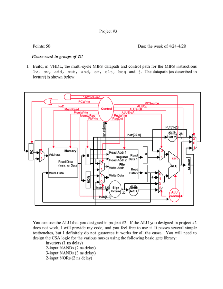
Project #3 Points: 50 Due: the week of 4/24-4/28 Please work in groups of 2!! 1. Build, in VHDL, the multi-cycle MIPS datapath and control path for the MIPS instructions lw, sw, add, sub, and, or, slt, beq and j. The datapath (as described in lecture) is shown below. PCWriteCond PCWrite PCSource ALUOp Control MemRead ALUSrcB MemWrite ALUSrcA MemtoReg RegWrite IRWrite RegDst 0 1 MDR Write Data 1 Read Register Read Addr 2 Data 1 File Write Addr Write Data 1 zero ALU Read Data 2 4 0 Instr[15-0] Sign Extend 32 Instr[5-0] 2 0 1 Shift left 2 ALUout Read Data (Instr. or Data) 28 0 Read Addr 1 1 Shift left 2 Instr[25-0] A Memory Address IR PC Instr[31-26] 0 PC[31-28] B IorD 0 1 2 3 ALU control You can use the ALU that you designed in project #2. If the ALU you designed in project #2 does not work, I will provide my code, and you feel free to use it. It passes several simple testbenches, but I definitely do not guarantee it works for all the cases. You will need to design the CSA logic for the various muxes using the following basic gate library: inverters (1 ns delay) 2-input NANDs (2 ns delay) 3-input NANDs (3 ns delay) 2-input NORs (2 ns delay) 3-input NORs (3 ns delay) 2-input XORs (3 ns delay). You may use process based code for the negative edge triggered registers (PC, IR, MDR, A, B, and ALUout – all of which you should initialize to zero at the beginning of the simulation) using a 10 ns read delay and a 0 ns write delay. You should also use process based code for the Control unit using a 20 ns control signal output delay (see Section 4.8 in Yalamanchili for the way to design both Mealy and Moore finite state machines) and for the Clock (see Section 4.6 in Yalamanchili for the way to generate a clock signal). Sign Extend and Shift left 2 can be handled easily in the port map structural descriptions that interconnect components and thus incur no delay. You will be provided with the code for the Register File and for a test Memory. Thus, most of your job will be to correctly connect your various components via port maps and design the Control (Moore style) finite state machine. The VHDL for the Register File shown below will be provided on the course web page. Note that Register File writes occur on a negative transition of reg_write with a 0 ns delay and that reads have a delay of 50 ns. Also note that the value stored in all registers is initialized to 0. library IEEE; use IEEE.std_logic_1164.all; use IEEE.std_logic_unsigned.all; entity RegFile is port(write_data: in std_logic_vector(31 downto 0); write_addr, read1_addr, read2_addr: in std_logic_vector(4 downto 0); reg_write: in std_logic; read1_data, read2_data: out std_logic_vector(31 downto 0)); end RegFile; architecture RegFile_behavior of RegFile is type reg_array is array(0 to 31) of std_logic_vector (31 downto 0); begin RegFile_process: process(read1_addr, read2_addr, reg_write) variable data_array: reg_array := ( (X”00000000”), -- $zero (X”00000000”), -- $at . . . (X”00000000”)); -- $ra variable addrofread1, addrofread2, addrofwrite: integer; begin addrofread1 := conv_integer(read1_addr); addrofread2 := conv_integer(read2_addr); addrofwrite := conv_integer(write_addr); if (reg_write’event and reg_write = ‘0’) then if (addrofwrite /= 0) then data_array(addrofwrite) := write_data; end if; end if; read1_data <= data_array(addrofread1) after 50 ns; read2_data <= data_array(addrofread2) after 50 ns; end process RegFile_process; end RegFile_behavior; The VHDL for the Memory shown on the next page will also be provided on the course web. [A similar (but not identical) Memory will be used when grading your assignment.] Note that the Memory is only 32 words (128 bytes) big (leaving space for 16 instructions in the lower half and 16 words of data in the upper half). The mux feeding the Memory should only connect to the Memory addr input the least significant 7 bits from either the PC or ALUout. Note that Memory writes occur on a negative transition of mem_write with a 0 ns delay and that reads have a delay of 100 ns. You will probably want to “disassemble” the instructions (turn then back into MIPS assembler code) to determine what the code is doing so you can check to make sure your VHDL implementation is working correctly. library IEEE; use IEEE.std_logic_1164.all; use IEEE.std_logic_unsigned.all; entity Memory is port(write_data: in std_logic_vector(31 downto 0); addr: in std_logic_vector(6 downto 0); mem_read, mem_write: in std_logic; read_data: out std_logic_vector(31 downto 0)); end Memory; architecture Memory_behavior of Memory is type mem_array is array(0 to 31) of std_logic_vector (31 downto 0); begin Memory_process: process(addr, mem_write) variable data_array: mem_array := ( (X”00004020”), (X”8D090040”), (X”8D0A0044”), (X”8D040048”), (X”0124582A”), (X”11600003”), (X”01094020”), (X”012A4820”), (X”08000004”), (X”AD48004A”), (X”01284022”), (X”AD48004E”), (X”01284024”), (X”AD480052”), (X”00000000”), (X”00000000”), (X”00000001”), (X”00000002”), (X”00000006”), (X”00000000”), (X”00000000”), (X”00000000”), (X”00000000”), (X”00000000”), (X”00000000”), (X”00000000”), (X”00000000”), (X”00000000”) (X”00000000”), (X”00000000”), (X”00000000”), (X”00000000”)); variable word_addr: integer; begin word_addr := conv_integer(addr(6 downto 2)); if (mem_write’event and mem_write = ‘0’) then data_array(word_addr) := write_data; end if; if (mem_read = ‘1’) then read_data <= data_array(word_addr) after 100 ns; end process Memory_process; end Memory_behavior; How fast could your run your clock; and, thus, what is the MHz rating of your machine? How many cycles did the code take to run (you should stop simulating when the next instruction fetched is a noop (all zeros))? At most two students can work in a group. Each group only need to submit one solution. Your code will be re-analyzed (vhdlan) and re-simulated (vhdlsim) using a different Memory as part of the grading process. Be sure to use the exact entity definition and architecture name for the sample Memory as the grading versions will use the same interface as well.

