Lecture 9/24/03
advertisement
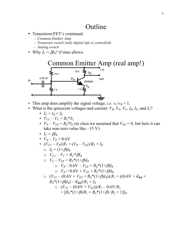
1 Outline • Transistors/FET’s continued – Common Emitter Amp – Transistor switch (only digital info is controlled) – Analog switch • Why IC = βIB? if time allows. Common Emitter Amp (real amp!) • This amp does amplify the signal voltage, i.e. vC/vB > 1. • What is the quiescent voltages and current: VB, VE, VC, IB, IE, and IC? • IC + IB = IE • VCC – VC = RC*IC • VE – VEE = RE*IE (in class we assumed that VEE = 0, but here it can take non-zero value like –15 V) • I C = βI B • VB – VE = 0.6V • (VCC – VB)/R1 = (VB – VEE)/R2 + IB o IE = (1+β)IB o VCC – VC = RC*βIB o VE – VEE = RE*(1+β)IB o VB – 0.6V – VEE = RE*(1+β)IB o VB = 0.6V + VEE + RE*(1+β)IB o (VCC – (0.6V + VEE + RE*(1+β)IB))/R1 = ((0.6V + VEE + RE*(1+β)IB) – VEE)/R2 + IB o (VCC – (0.6V + VEE))/R1 – 0.6V/R2 = [RE*(1+β)/R1 + RE*(1+β) /R2 + 1]IB 2 VCC − 0.6 − VEE 0.6 − (V − 0.6 − VEE ) R2 − 0.6 R1 R1 R2 o IB = = CC = RE (1 + β ) RE (1 + β ) R ( 1 + β )( R + R ) + R R E 1 2 1 2 + +1 R1 R2 (VCC − VEE ) R2 − 0.6( R1 + R2 ) R1R2 ] RE (1 + β )[( R1 + R2 ) + RE (1 + β ) (VCC − VEE ) R2 − 0.6( R1 + R2 ) ≈ R1R2 RE (1 + β )( R1 + R2 )[1 + ] RE (1 + β )( R1 + R2 ) (VCC − VEE ) R2 R1R2 0.6 ≈ [1 − ]− RE (1 + β )( R1 + R2 ) RE (1 + β )( R1 + R2 ) RE (1 + β ) (V − 0.6 − VEE ) R2 − 0.6 R1 or alternatively, CC = RE (1 + β )( R1 + R2 ) + R1R2 (VCC − VEE ) R2 − 0.6 V − (0.6 + VEE ) R1 + R2 = 0 ' , where R1R2 R + R // R E 1 2 RE (1 + β ) + ( R1 + R2 ) (V R + VEE R1 ) V0 ≡ CC 2 and RE' ≡ RE (1 + β ) R1 + R2 V − (0.6 + VEE ) o VB = 0.6V + VEE + RE*(1+β) 0 ' RE + R1 // R2 V − (0.6 + VEE ) = 0.6 + VEE + RE' 0 ' RE + R1 // R2 ' ' ' = REV0 − RE (0.6 + VEE ) + (0.6 + VEE )( RE + R1 // R2 ) RE' + R1 // R2 ' = REV0 + (0.6 + VEE )( R1 // R2 ) RE' + R1 // R2 o IC = β*IB = β V0 − (0.6 + VEE ) RE' + R1 // R2 o VC = VCC – RC*IC = VCC − RC = V0 − (0.6 + VEE ) 1+ β R // R2 RE β + 1 β V0 − (0.6 + VEE ) 1+ β RE β + R1 // R2 β 3 • Or in a more intuitive fashion, • From the base side, 1k connected to the emitter is the same as multiplied by β, so it is much larger than the 1k on the base, and negligible. So VB is15 V divided by 10k and 1k ~ 1.36 V. • Then VE is lower by 0.6 V → 0.76 V. • IE must then be 0.76V/1k = 0.76 mA. • IC must then be also 0.76 mA (ignoring 1/β difference) • VC must then be 0.76 mA*10kΩ lower than 15 V → 15 – 7.6 = 7.4 V. • IB must be 0.76 mA/β = 7.6 µA. Since the voltage divider on the base has current of 15/11k = 1.36mA, this 7.6 µA is small enough to be neglected. • When an AC voltage, ∆v, is applied, at the input, what is the AC voltages and currents vB, vE, vC, iB, iE, and iC? What is the gain of this amp? (Assume that freq is “high enough”) • (IC+iC)+ (IB+iB) = (IE+iE) but since already IC + IB = IE, iC + iB = iE. • VCC – (VC+vC) = RC*(IC+iC) but since already VCC – VC = RC*IC so –vC = RC*iC • Similarly, • vE = RE*iE • iC = βiB • vB – vE = 0 • – vB/R1 = vB/R2 + iB won’t hold since the change in vB is caused by changing current flowing into the base. o vB = vE = RE*iE = RE*(1+β)iB o vC = –RC*iC = –RC*βiB = –RC*βiB = –RC*βvB/ RE*(1+β) ~ –(RC/RE)vB • Or in more intuitive fashion, • vB = vE = ∆v, iE = iC = ∆v /1k. Then vC = ∆v /1k*10k = 10∆v. • So the gain must be 10. • Note that since VE = 0.8V, vE cannot go down more than 0.8V. • Similarly, vC cannot go up 8 V or go down by 7 V. • What is the input and output impedance of this circuit (for AC)? • Input impedance is similar to the emitter follower: inherent input impedance is (1+β)*1k (in emitter). But 10k and 1k connected from input (to ground and 15V) act as input impedance (in parallel), which actually dominate the net impedance. So it is about 1k (slightly less). • Zin = vB/iin, where iin is iB + i2 + i1 = vB/RE*(1+β) + vB/R2 + vB/R1. So 4 • Zin = vB/iin = (1/RE*(1+β) + 1/R1 + 1/R2)-1 = R’E// R1//R2. • Output impedance is RC [and v0 = vin*(RC/ RE)].
