Bipolar Junction Transistors
advertisement
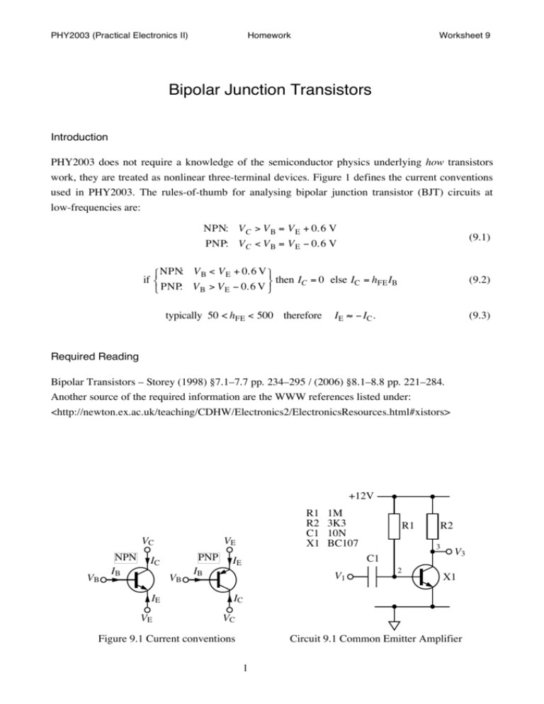
PHY2003 (Practical Electronics II) Homework Worksheet 9 Bipolar Junction Transistors Introduction PHY2003 does not require a knowledge of the semiconductor physics underlying how transistors work, they are treated as nonlinear three-terminal devices. Figure 1 defines the current conventions used in PHY2003. The rules-of-thumb for analysing bipolar junction transistor (BJT) circuits at low-frequencies are: NPN: V C > V B = V E + 0.6 V (9.1) PNP: V C < V B = V E ! 0.6 V " NPN: V B < V E + 0.6 V % if # & then IC = 0 else IC = hFE IB $ PNP: V B > V E ! 0.6 V ' typically 50 < hFE < 500 therefore (9.2) IE ! " IC . (9.3) Required Reading Bipolar Transistors – Storey (1998) §7.1–7.7 pp. 234–295 / (2006) §8.1–8.8 pp. 221–284. Another source of the required information are the WWW references listed under: <http://newton.ex.ac.uk/teaching/CDHW/Electronics2/ElectronicsResources.html#xistors> +12V VC VB NPN IB VE PNP IC VB IE VE R1 R2 C1 X1 IB 1M 3K3 10N BC107 R1 3 C1 IE V1 R2 2 V3 X1 IC VC Figure 9.1 Current conventions Circuit 9.1 Common Emitter Amplifier 1 PHY2003 (Practical Electronics II) Homework Worksheet 9 12V R1 C1 R3 4 V1 2 C1 R1 R2 R3 R4 X1 0µ1 33K 10K 2K7 1K0 BC107 V4 X1 3 R2 R4 Circuit 9.2 Series Feedback Amplifier Exercise 9.1 Analyse circuit 9.1 using typical values from the BC107 datasheet and find: (a) the quiescent voltage at node 3, (b) the DC impedance of node 2 and hence the low-frequency –3 dB point (c) the small-signal voltage gain v3 v1 at 1 kHz and 10 kHz. Answers: (a) 6.4 V (assuming HFE = 150) (b) 2.2 k!, 7.2 kHz (c) –60 and –400 Exercise 9.2 Analyse circuit 9.2 using typical values from the BC107 datasheet and find: (a) the quiescent voltage at node 3 (b) the quiescent voltage at node 4 (c) the small-signal gain v 4 v1 at 1kHz Answers: (a) 2.1 V (b) 6.3 V (b) –60 and –400 (c) v 4 v1 = !2.7 © Copyright CDH Williams University of Exeter 2006 CW061019/5 2
