TN-41-02: DDR3 ZQ Calibration
Introduction
Technical Note
DDR3 ZQ Calibration
Introduction
For more robust system operation, the DDR3 SDRAM driver design has been enhanced
with reduced capacitance, dynamic on-die termination (ODT), and a new calibration
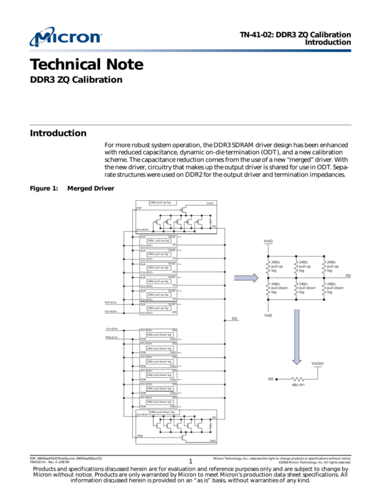
scheme. The capacitance reduction comes from the use of a new “merged” driver. With
the new driver, circuitry that makes up the output driver is shared for use in ODT. Separate structures were used on DDR2 for the output driver and termination impedances.
Figure 1:
Merged Driver
240Ω pull-up leg
VDDQ
PUP
DQ
VOH<0:4>
VDDQ
PUP
240Ω pull-up leg
VDDQ
DQ
VOH<0:4>
VDDQ
PUP
240Ω pull-up leg
DQ
VOH<0:4>
VDDQ
PUP
240Ω pull-up leg
DQ
VOH<0:4>
240Ω
pull-up
leg
240Ω
pull-up
leg
240Ω
pull-down
leg
240Ω
pull-down
leg
240Ω
pull-down
leg
DQ
VDDQ
PUP
240Ω pull-up leg
DQ
VOH<0:4>
VDDQ
PUP
240Ω pull-up leg
DQ
VOH<0:4>
PUP<0:3>
240Ω
pull-up
leg
VDDQ
PUP
240Ω pull-up leg
VOH<0:4>
DQ
VOH<0:4>
DQ
VOL<0:4>
VOL<0:4>
VSSQ
DQ
240Ω pull-down leg
PDN<0:3>
PDN
VSSQ
VOL<0:4>
DQ
240Ω pull-down leg
PDN
VSSQ
DQ
VOL<0:4>
240Ω pull-down leg
PDN
VDDQ/2
VSSQ
VOL<0:4>
DQ
240Ω pull-down leg
PDN
DQ
VSSQ
VOL<0:4>
DQ
40Ω RTT
240Ω pull-down leg
PDN
VSSQ
VOL<0:4>
DQ
240Ω pull-down leg
PDN
VOL<0:4>
VSSQ
240Ω pull-down leg
DQ
PDN
VSSQ
PDF: 09005aef83207fed/Source: 09005aef82eccf52
TN4102.fm - Rev. A 2/08 EN
1
Micron Technology, Inc., reserves the right to change products or specifications without notice.
©2008 Micron Technology, Inc. All rights reserved.
Products and specifications discussed herein are for evaluation and reference purposes only and are subject to change by
Micron without notice. Products are only warranted by Micron to meet Micron’s production data sheet specifications. All
information discussed herein is provided on an “as is” basis, without warranties of any kind.
TN-41-02: DDR3 ZQ Calibration
Calibration Method
The concept of the merged driver uses multiple 240Ω structures to enable the pull-up
and pull-down networks (see Figure 1 on page 1). Multiple termination values are realized by enabling different combinations of the same 240Ω structures. For DDR3, the
output impedance of the full-strength driver is 34Ω by default and is obtained by
enabling all seven of the 240Ω legs.
To accomplish the data rates exclusive to DDR3, special attention must be paid to signal
integrity. Minimizing any impedance mismatch on the traces connecting the memory
controller to the DRAM outputs will help reduce reflections and ringing on the signals.
To help reduce these impedance discontinuities, a precision calibration scheme is introduced in DDR3.
Calibration Method
The ZQ calibration in DDR3 is used both for the output driver and the ODT. The ZQ ball
of each DRAM is connected to an external precision (±1%) 240Ω resistor. This resistor
may be shared among devices as long as the controller does not overlap any timing associated with the calibration and as long as the capacitive loading does not exceed specification.
Figure 2:
Pull-Up Calibration
240Ω pull-up driver
VDDQ
PUP
VOH<0:4>
VOL<0:4>
DQ calibration
control block
VOH<0:4>
Enter cal.
Exit cal.
VPULL-UP
DQ
XRES
240Ω
external
resistor
VDDQ/2
The calibration control block consists of an analog-to-digital converter (ADC), comparators, a majority filter, an internal reference voltage generator, and an approximation
register. The 240Ω legs in the calibration control block are matched to the pull-up legs
used in the output driver and termination options. The pull-up leg uses a polyresistor
that is slightly larger than 240Ω. It employs several P-channel devices to reduce the resistance of the legs and to tune the polyresistor to 240Ω. This resistor is used to archive a
more linear pull-up and pull-down curve for improved signal integrity at the system
level. The pull-down leg is similar to the pull-up leg. It uses a large polyresistor with
multiple N-channel devices for tuning.
When a ZQ calibration command is given, the pull-up line is driven LOW, and the pullup leg is pulled to VDDQ. The voltage pull-up (VPULL-UP) line is used to compare the
voltage at the XRES point to an internally generated reference voltage (VDDQ/2) by using
the comparator inside the DQ calibration control block. The P-channel tuning devices
are individually tuned using the VOH signals until the voltage at XRES equals the internally generated reference voltage (VDDQ/2). The VOH codes are stored in the internal
approximation register and sent to each of the pull-up legs of the output drivers and
termination. After all the pull-up devices have been calibrated to the external resistor,
the comparator is again used to compare the voltage on the pull-down (VPULL-DOWN)
PDF: 09005aef83207fed/Source: 09005aef82eccf52
TN4102.fm - Rev. A 2/08 EN
2
Micron Technology, Inc., reserves the right to change products or specifications without notice.
©2008 Micron Technology, Inc. All rights reserved
TN-41-02: DDR3 ZQ Calibration
ZQ Calibration Commands
line to the reference voltage set at VDDQ/2. This process generates the VOL codes and
updates the pull-down devices at the appropriate time, completing the calibration
process.
ZQ Calibration Commands
Two new commands relating to ZQ calibration are introduced in DDR3. The ZQ CALIBRATION LONG (ZQCL) command is most often used at initial system power-up or
when the device is in a reset condition. The ZQCL command resolves the problem of
manufacturing process variation and calibrates the DRAM to an initial temperature and
voltage setting. A full calibration using the ZQCL command takes 512 clock cycles to
complete. During this calibration time, the memory data bus must remain completely
idle and quiet. Any time the DRAM is idle after the initial calibration, subsequent ZQCL
commands may be issued. For these subsequent commands (commands issued at times
other than initialization and reset), the timing window required to complete the calibration is reduced to 256 clock cycles.
The ZQ CALIBRATION SHORT (ZQCS) command tracks the continuous voltage and
temperature changes associated with normal operation. Periodic short calibrations
enable the DRAM to maintain linear output driver and termination impedance over the
full voltage and temperature range. A ZQCS command takes 64 clock cycles to complete.
Table 1:
ZQ Command Truth Table
CKE
Function
Previous Next
Abbreviation
Cycle
Cycle
CS# CAS# RAS#
WE#
BA0–
BA3
A13–
A15
A12
A10
A0–
A9,
A11
ZQ CALIBRATION
LONG
ZQCL
H
H
L
H
H
L
X
X
X
H
X
ZQ CALIBRATION
SHORT
ZQCS
H
H
L
H
H
L
X
X
X
L
X
ZQ Calibration Timing
The first ZQCL issued after RESET must be given a timing period of tZQINIT (512 clock
cycles) to perform the full calibration. A timing period of tZQOPER (256 clock cycles) must
be allowed for any subsequent ZQCL commands. The ZQCL command may be used any
time there is more impedance error than can be corrected with a ZQCS command.
Again, during the tZQINIT and tZQOPER time windows, the DRAM channel must remain
completely quiet.
ZQCS commands may be issued any time the DRAM is not performing activities. A
shorter timing window of 64 clocks (tZQCS) must be satisfied before normal operation
may resume.
All banks must be precharged and tRP met before any calibration commands may be
issued by the controller (see Figure 3 on page 4). ZQCL or ZQCS commands may be
issued inside of t XSDLL time when exiting self refresh. An explicit calibration command
must be issued upon self refresh exit for the I/O calibration to take place. After self
refresh exit, tXS must be satisfied before either ZQCL or ZQCS is issued.
PDF: 09005aef83207fed/Source: 09005aef82eccf52
TN4102.fm - Rev. A 2/08 EN
3
Micron Technology, Inc., reserves the right to change products or specifications without notice.
©2008 Micron Technology, Inc. All rights reserved
TN-41-02: DDR3 ZQ Calibration
Calculating the Calibration Interval
Figure 3:
ZQ Calibration Timing
T0
T1
Ta0
Ta1
Ta2
Ta3
Tb0
Tb1
Tc0
Tc1
Tc2
ZQCL
NOP
NOP
NOP
Valid
Valid
ZQCS
NOP
NOP
NOP
Valid
Address
Valid
Valid
Valid
A10
Valid
Valid
Valid
CK#
CK
Command
CKE
(1)
Valid
Valid
(1)
Valid
ODT
(2)
Valid
Valid
(2)
Valid
Activities
(3)
DQ bus
(3)
High-Z
tZQINIT
or tZQOPER
High-Z
Activities
tZQCS
Time Break
Notes:
Don’t Care
1. CKE must be continuously registered HIGH during the calibration procedure.
2. ODT must be disabled via the ODT signal or the MRS command during the calibration procedure.
3. All devices connected to the DQ bus should be High-Z during the calibration procedure.
Calculating the Calibration Interval
The frequency of ZQ calibration commands will be dependent on system temperature
and voltage drift rates. To maintain the linear output driver and termination impedances, the controller will need to issue ZQCS commands at specific intervals to account
for slight system environment changes.
One method for determining these timing intervals is to use the temperature
(Tdriftrate) and the voltage (Vdriftrate) drift rates that the DRAM is subjected to in the
application. Along with the system-specific drift rates, the design should assume
maximum ODT voltage and temperature sensitivities taken from the DDR3 specification, as shown in Table 2.
Table 2:
ODT Voltage and Temperature Sensitivity
Change
Min
Max
Units
dRTTdT
0
1.5
%/°C
dRTTdV
0
0.15
%/mV
The DRAM is capable of correcting 0.5% impedance error within a 64 clock period
(ZQCS command period). This number, along with the system drift rates, can be used in
the formula below to calculate the calibration interval.
0.5%
--------------------------------------------------------------------------------------------------------------( Tsens × Tdriftrate ) + ( Vsens × Vdriftrate )
Note:
PDF: 09005aef83207fed/Source: 09005aef82eccf52
TN4102.fm - Rev. A 2/08 EN
Tsens and Vsens are the maximum temperature and voltage sensitivities taken from
Table 2. Values are for illustration purposes only. Refer to the component data sheet
for current specifications.
4
Micron Technology, Inc., reserves the right to change products or specifications without notice.
©2008 Micron Technology, Inc. All rights reserved
TN-41-02: DDR3 ZQ Calibration
Conclusion
Example Calculation
From the system environment:
Tdriftrate = 1.2°C/s
Vdriftrate = 10 mV/s
From the specifications in Table 2 on page 4:
Tsens = 1.5%/°C
Vsens = .15%/mV
0.5%
Time between ZQCS commands = -----------------------------------------------------------------------------------1.2°C
.15% 10mV
⎛ 1.5%
------------ × -------------⎞ + ⎛ ------------ × ---------------⎞
⎝ °C
1s ⎠ ⎝ mV
1s ⎠
0.5%
= -----------------------------------------1.8%
⎛ ------------⎞ + ⎛ 1.5%
------------⎞
⎝ 1s ⎠ ⎝ 1s ⎠
0.5%
= --------------------- = .152s = 152ms
3.3% ⁄ 1s
To maintain RON and ODT accuracy, the maximum amount of time between ZQCS
commands would be 152ms for the system in the example. To determine the number of
clocks, divide by tCK.
Conclusion
The DDR3 ZQ calibration scheme provides an improvement in controlled impedance
values and significantly tighter tolerances when compared with DDR2. The long calibration at initialization enables the DRAM to minimize any process variation present in the
driver. Short calibrations during normal operation reduce impedance variation due to
voltage and temperature drift. This accuracy helps to minimize impedance discontinuities between PCB trace and driver and improves overall signal integrity.
8000 S. Federal Way, P.O. Box 6, Boise, ID 83707-0006, Tel: 208-368-3900
prodmktg@micron.com www.micron.com Customer Comment Line: 800-932-4992
Micron, the M logo, and the Micron logo are trademarks of Micron Technology, Inc. All other trademarks are the property of their respective owners.
PDF: 09005aef83207fed/Source: 09005aef82eccf52
TN4102.fm - Rev. A 2/08 EN
5
Micron Technology, Inc., reserves the right to change products or specifications without notice.
©2008 Micron Technology, Inc. All rights reserved.


