www.embedinfo.com/en
www.embedinfo.com/en
Emlink ICE for VDSP++
Emlink ICE for Blackfin JTAG Adapter
User's Getting Started
Getting Started
EMLINK-BH Features:
Revision 2.1.0825, August 2008
Part Number: EDT-EMLINK-GS
♦ Compatible with ADI VisualDSP++ 3.5/4.0/4.5/5.0 IDDE
♦ Supports Blackfin processors, BF531/2/3/4/6/7 etc.
Embest Info & Tech Co., LTD
Rm509, Luohu Science & Tech Bldg 85# Taining Road
Shenzhen, China 518020
Tel: +86 755 25621715
Fax: +86 755 25616057
♦ Debugging with Halt, Step, Run, Breakpoint
Copyright Information
♦ JTAG port (20pins, FH2.54mm) for connecting target board
♦ Supports Windows98/NT/2000 /XP host
♦ Support USB 2.0 protocol
♦ Mini and smart size: 45x32x12mm, weight about 55g
♦ Power suply via USB port without power adapter
© 2008 Embest, ALL RIGHTS RESERVED. This document may not be reproduced in any form
without prior, express written consent from Embest.
♦ Downloading and debugging speed up to 200KBytes/s (1.5Mbps)
♦ Support to program on-board Flash.
Printed in the China.
Emlink ICE for Blackfin (Type: EMLINK-BH)
Limited Warranty
The USB-based adapter hardware is warranted against defects in materials and workmanship for a
period of one year from the date of purchase from Embest or from an authorized dealer.
Disclaimer
Embest reserves the right to change this product without prior notice. Information furnished by
Embest is believed to be accurate and reliable. However, no responsibility is assumed by Embest
for its use, nor for any infringement of patents or other rights of third parties which may result
from its use. No license is granted by implication or otherwise under the patent rights of Embest
Trademark and Service Mark Notice
The Analog Devices logo, Blackfin, the Blackfin logo, VisualDSP, the VisualDSP logo, EZ-KIT
Lite logo, and EZ-ICE are registered trademarks are registered trademarks of Analog Devices, Inc.
VisualDSP++, the VisualDSP++ logo, ICEPAC, and The DSP Collaborative are trademarks of
Analog Devices, Inc.
Emlink ICE, the Emlink logo are trademarks of Embest Info & Tech Co., LTD.
All other brand and product names are trademarks or service marks of their respective owners.
Regulatory Compliance
The USB based adapter is designed to be used solely in a laboratory environment. The adapter is
not intended to be used in any end products or as a portion of an end product. The adapter may
cause interference to other electronic devices operating at close proximity. The adapter should not
be used in or near any medical equipment or RF devices.
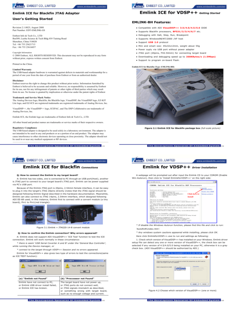
Figure 2.1 Emlink ICE for Blackfin package box (full-scale picture)
1/8
2/8
www.embedinfo.com/en
Emlink ICE for Blackfin
www.embedinfo.com/en
Emlink for VDSP++
Connections
Q: How to connect the Emlink to my target board?
A: Emlink has two sides, one is connected to PC through an USB port(Host), another
is JTAG port to connect to your target board’s JTAG port. Emlink can be power supplied
via PC’s USB port.
Driver Installation
A webpage will be prompted out after input the Emlink CD to your CDROM (Enable
Win-Autorun), then click to ‘Install EmlinkforVDSP++’ on the right side:
Because of the Emlink JTAG port is 20pins, 2.54mm female interface, it can be easy
to plug it into the target’s JTAG 20pins directly (notes that the JTAG signal should be
designed following Emlink Signal described in the hardware documentation. Meanwhile,
Emlink can also connect to JTAG 14pins, 2.54mm interface, which designed following
ADI EE-68 used, in this instance, Emlink first to connect with a convert module (a tiny
board), Pin1 to Pin1(red triangle):
Click here to
Install
* If disable the Windows Autorun function, please find this file and click to run:
Figure 3.1 Emlink + JTAG20-14-8 convert module
‘AutoRUN\index.htm’.
* Any windows system cautions appeared while installing, please click OK.
Q: How to confirm the Emlink connection? Why errors appeared?
A: Emlink does not support ADI VisualDSP++ ‘ICE Test’ function to test the ICE
connection. Emlink will work normally in these circumstance:
* there is seem ‘USB Serial Coverter A and B’ under the ‘General Bus Controller’,
while running the Device manager, or
* connect to the target through VDSP++ Session and no errors appeared.
Here click EmlinkforVDSP++.exe to run and settings as following:
1. Check which version of VisualDSP++ has installed on your Windows. Emlink driver
setup file can detect any one or more version of VisualDSP++, the check box can be
selected if any version of 4.5/4.0/5.0 being installed on your PC, otherwise it is a gray
check box. (ADI VisualDSP++ should be authorized by ADI.)
Emlink for VisualDSP++ also gives two type of errors to test the connections(same
as ICE TEST function):
(a) “Emlink not Found”
(b) “Proccessor not Found”
Emlink have not connect to PC,
or Emlink USB driver install failed,
or Emlink ICE has broken.
The target board have not power up,
or JTAG ports do not connect well,
or JTAG signals mismatch as described,
or something wrong with target board,
such as no enough voltage and current.
3/8
Figure 4.2 Choose which version of VisualDSP++ (one or more)
4/8
www.embedinfo.com/en
www.embedinfo.com/en
2. If one or more version of VisualDSP++ can be select, click ‘Install’ to continue, the
prompt out window as following:
Emlink for VDSP++
Screen Shots and FAQs
☼
Emlink driver for VisualDSP++ setup process is easy to understand: click EmlinkforVDSP++.exe to run,
then the driver could be installed on the Windows system, the ‘Legacy target’ should be available to select.
After a while, the Emlink USB driver should be installed to your windows, and display
message such as: ‘…Process completed.’, then press Enter to finish, show as figure
5.2(a). The setup program will go on to copy and install Emlink driver for VDSP++. If the
last message gives out: ‘Completed’, installation has success and finish, show as figure
5.2(b).
Figure 6.1 Emlink for VDSP++ Connection Type
☼ Emlink ICE for Blackfin can use to debug BF531/2/3/4/6/7 target: debug source code in RAM or trace in
Flash.
Completed
Figure 5.2 (a) press Enter to exit USB installation
(b) install completed and all 100%
3. Create a new Session under VisualDSP++ 4.5/4.0/5 to check if the
EmlinkforVDSP++.exe installed success or not. If the installation was correct, the
reserved device ‘Legacy target’ was available (can be selected) as following.
Otherwise, the ‘Legacy target’ could not be selected (gray) if the Emlink driver install
failed.
Figure 6.2 Session for BF53X + Emlink
☼ NOTES: ADI VisualDSP++ 4.0/4.5/5.0 are the commercial products provide by ADI,
customer should be authorized by ADI before using Emlink to debug your system.
Figure 5.3 (a)Emlink target selection for VDSP++ Session
(b)Emlink device
NOTES: If the Emlink USB driver installed failed, the error ‘0x80004005’ will be
appeared while connect Emlink to your target. Please check them like Figure 5.3.
5/8
6/8
www.embedinfo.com/en
Emlink ICE for Blackfin
Hardware description
Features:
♦ Compatible with ADI VisualDSP++ 4.0/4.5/5.0 IDDE
♦ Supports Blackfin BF53x processors, BF531/2/3/4/6/7 etc.
♦ Debugging with Halt, Step, Run, Breakpoint
♦ Supports Windows98/NT/2000 /XP host
♦ Support USB 2.0 protocol
♦ Mini and smart size: 45x32x12mm, weight about 55g
♦ Power suply via USB port without power adapter
♦ JTAG port (20pins, FH2.54mm) for connecting target board
♦ Downloading and debugging speed up to 200KBytes/s (1.5Mbps)
♦ Support to program on-board Flash.
Embest Emlink ICE for Blackfin DSP
Hardware signals and ports
Emlink has two sides, one is connected to PC through an USB port(Host), another is
JTAG port to connect to your target board’s JTAG port. Emlink can be power supplied via
PC’s USB port.
JP1_S
J1
TMS
TDO
TDI
TCK
nTRST
EMU
GND
Vsupply
1
2
3
4
5
6
7
8
DSP8
Vref
nTRST
TDI
TMS
TCK
TDO
nSRST
EMU
1
3
5
7
9
11
13
15
17
19
2
4
6
8
10
12
14
16
18
20
ARM10X2
Vsupply
GND
GND
GND
GND
GND
GND
GND
GND
JTAG20-14-8 Module
www.embedinfo.com/en
Signal
Type
Description
TRST
Test Reset (JTAG): Resets the test state machine. The TRST signal must be
Input
asserted after power up to ensure proper JTAG operation. The TRST signal has a
Asynchronous 10 Kohm internal pull-up resistor. Please do not pulled down with resistor on
this pin in board side, but let it open or pulled download >10Kohm.
TCK
Input
Test Clock (JTAG): Provides an asynchronous clock for JTAG boundary scan.
TDI
Input
Test Data Input (JTAG): A serial data input of the boundary scan path. This
signal has a 10 kW internal pull-up resistor.
TDO
Output
Test Data Output (JTAG): A serial data output of the boundary scan path.
TMS
Input
Test Mode Select (JTAG): Controls the test state machine. This signal has a
10 kW internal pull-up resistor.
nSRST Input
The target system reset signal. ICE can reset target via this signal.
NC
X
No connect on Emlink side.
GND
X
Ground.
RES
X
Reserved.
Refer to the IEEE 1149.1 JTAG specification for detailed information on the JTAG
interface. This document assumes a working knowledge of the JTAG specification.
JP3_D
GND
1
3
5
7
9
11
13
GND
EMU
GND
TMS
TCK
nTRST
TDI
TDO
2
4
6
8
10
12
14
Power supply
Emlink can be power supplied via PC USB, without any power adapter.
DSP7X2
Emlink JTAG 20pins
Emlink Connect Target
Figure 7.2 Emlink JTAG signal definition and connection
NOTES for JTAG signal designed:
- It is recommended to design your target board as 20pins, then Emlink
can be plugged in directly.
- If designed to other pins (only connect the active signals’ pin), then
user has to connect correct signal to Emlink JTAG port.
Figure 8.1 (a)Emlink target selection for VDSP++ Session
- There is 10Kohm resistor pulled up inside Emlink nTRST pin, please do
not pulled down with resistor this signal in board side (open or >10Kohm).
- All signal ‘GND’ should be connect to target board ground, 0V.
7/8
(b)Emlink device
NOTES: If the Emlink USB driver installed failed, the error ‘0x80004005’ will be
appeared while connect Emlink to your target. Please check and resolve by:
* check if there is ‘USB Serial Coverter A/B’ device under the list. if there is ? or ! on
them, please re-install EmlinkforVDSP++.exe again, and restart your windows once
after finished the installation, until there is no ‘?’ or ‘!’ on them. And the correct status of
these device show as figure 8.1(b).
8/8
