Infrared Thermal Measurements on Electronic Devices
advertisement
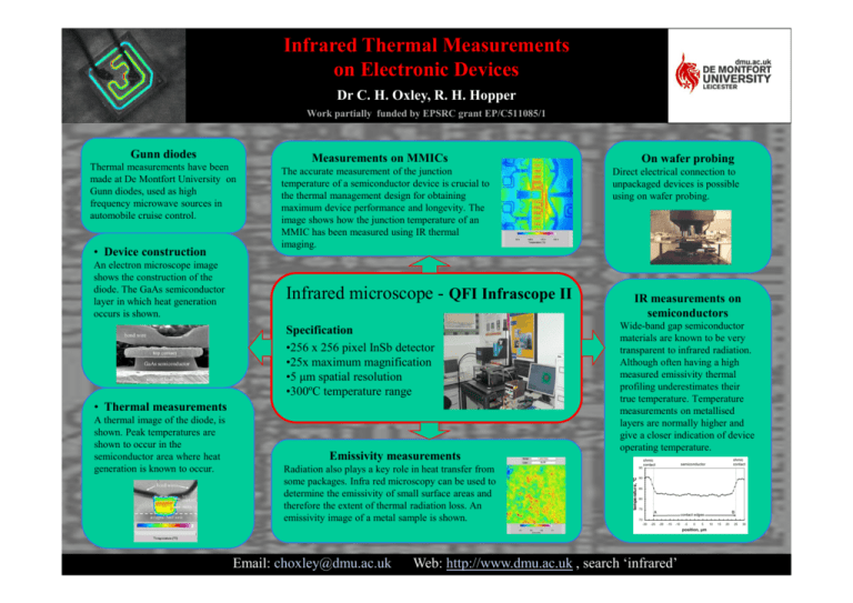
Infrared Thermal Measurements on Electronic Devices Dr C. H. Oxley, R. H. Hopper Work partially funded by EPSRC grant EP/C511085/1 • Device construction An electron microscope image shows the construction of the diode. The GaAs semiconductor layer in which heat generation occurs is shown. Measurements on MMICs The accurate measurement of the junction temperature of a semiconductor device is crucial to the thermal management design for obtaining maximum device performance and longevity. The image shows how the junction temperature of an MMIC has been measured using IR thermal imaging. Infrared microscope - QFI Infrascope II Specification •256 x 256 pixel InSb detector •25х maximum magnification •5 µm spatial resolution •300ºC temperature range • Thermal measurements A thermal image of the diode, is shown. Peak temperatures are shown to occur in the semiconductor area where heat generation is known to occur. Emissivity measurements Radiation also plays a key role in heat transfer from some packages. Infra red microscopy can be used to determine the emissivity of small surface areas and therefore the extent of thermal radiation loss. An emissivity image of a metal sample is shown. On wafer probing Direct electrical connection to unpackaged devices is possible using on wafer probing. IR measurements on semiconductors Wide-band gap semiconductor materials are known to be very transparent to infrared radiation. Although often having a high measured emissivity thermal profiling underestimates their true temperature. Temperature measurements on metallised layers are normally higher and give a closer indication of device operating temperature. 95 temperature, °C Gunn diodes Thermal measurements have been made at De Montfort University on Gunn diodes, used as high frequency microwave sources in automobile cruise control. ohmic contact 90 85 80 75 A B contact edges 70 -30 -25 -20 -15 -10 -5 0 5 position, µm Email: choxley@dmu.ac.uk ohmic contact semiconductor Web: http://www.dmu.ac.uk , search ‘infrared’ 10 15 20 25 30
