Design and Implementation of a LNA in UHF band using Microstrip
advertisement
Design and Implementation of a LNA
in UHF band using Microstrip
Rodríguez, Sebastián. Correa, Andrés. Fajardo, Arturo. Paez, Carlos
Department of Electronics
Pontificia Universidad Javeriana (PUJ)
Bogotá, Colombia
{ jrodriguezp, jairo.correa, fajardoa, paez.carlos }@javeriana.edu.co
Abstract— This article presents a design methodology for low
noise amplifiers (LNA) in the UHF band, optimized for
narrowband operation, based on a proper choice of the bias
operating point, modeling of the active element through S
parameters and the appropriate design of matching networks for
minimum noise figure and maximum gain under stable
conditions. Likewise, presents a case study related with the design
of an LNA with this methodology, together with the experimental
results and the results simulated with the Ansoft Designer®
platform.
Keywords-component; Design methodology,
Amplifier, Noise Figure, Amplifier Stability.
Low
Noise
I. INTRODUCTION
Most electronic applications of modern telecommunications are
focused on the ability to use the wireless environment as a clear
channel of communication. The reasons for the use of such
technologies are transparency to the user, portability and ubiquity.
The main application of low noise amplifiers (LNA) is to amplify the
signal received at the Radio Frequency (RF) front end [1-5] in the
receiver systems of the equipment, like cell phones where the signal
received is very low (typically in the range of -110 dBm and -70 dBm
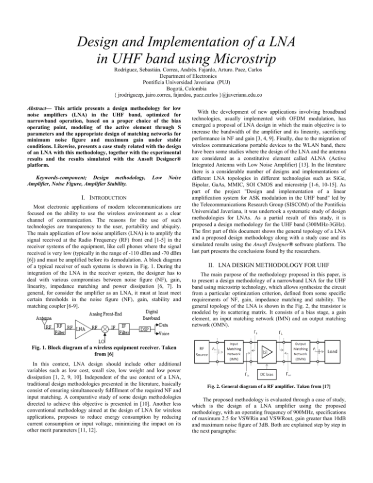
[6]) and must be amplified before its demodulation. A block diagram
of a typical receiver of such systems is shown in Fig. 1. During the
integration of the LNA in the receiver system, the designer has to
deal with various compromises between noise figure (NF), gain,
linearity, impedance matching and power dissipation [6, 7]. In
general, for consider the amplifier as an LNA, it must at least meet
certain thresholds in the noise figure (NF), gain, stability and
matching coupler [6-9].
With the development of new applications involving broadband
technologies, usually implemented with OFDM modulation, has
emerged a proposal of LNA design in which the main objective is to
increase the bandwidth of the amplifier and its linearity, sacrificing
performance in NF and gain [3, 4, 9]. Finally, due to the migration of
wireless communications portable devices to the WLAN band, there
have been some studies where the design of the LNA and the antenna
are considered as a constitutive element called ALNA (Active
Integrated Antenna with Low Noise Amplifier) [13]. In the literature
there is a considerable number of designs and implementations of
different LNA topologies in different technologies such as SiGe,
Bipolar, GaAs, MMIC, SOI CMOS and microstrip [1-6, 10-15]. As
part of the project "Design and implementation of a linear
amplification system for ASK modulation in the UHF band" led by
the Telecommunications Research Group (SISCOM) of the Pontificia
Universidad Javeriana, it was undertook a systematic study of design
methodologies for LNAs. As a partial result of this study, it is
proposed a design methodology for the UHF band (300MHz-3GHz).
The first part of this document shows the general topology of a LNA
and a proposed design methodology along with a study case and its
simulated results using the Ansoft Designer® software platform. The
last part presents the conclusions found by the researchers.
II. LNA DESIGN METHODOLOGY FOR UHF
The main purpose of the methodology proposed in this paper, is
to present a design methodology of a narrowband LNA for the UHF
band using microstrip technology, which allows synthesize the circuit
from a particular optimization criterion, defined from some specific
requirements of NF, gain, impedance matching and stability. The
general topology of the LNA is shown in the Fig. 2, the transistor is
modeled by its scattering matrix. It consists of a bias stage, a gain
element, an input matching network (IMN) and an output matching
network (OMN).
Fig. 1. Block diagram of a wireless equipment receiver. Taken
from [6]
In this context, LNA design should include other additional
variables such as low cost, small size, low weight and low power
dissipation [1, 2, 9, 10]. Independent of the use context of a LNA,
traditional design methodologies presented in the literature, basically
consist of ensuring simultaneously fulfillment of the required NF and
input matching. A comparative study of some design methodologies
directed to achieve this objective is presented in [10]. Another less
conventional methodology aimed at the design of LNA for wireless
applications, proposes to reduce energy consumption by reducing
current consumption or input voltage, minimizing the impact on its
other merit parameters [11, 12].
Fig. 2. General diagram of a RF amplifier. Taken from [17]
The proposed methodology is evaluated through a case of study,
which is the design of a LNA amplifier using the proposed
methodology, with an operating frequency of 900MHz, specifications
of maximum 2.5 for VSWRin and VSWRout, gain greater than 10dB
and maximum noise figure of 3dB. Both are explained step by step in
the next paragraphs:
1. Choice of transistor and choice of biasing. A first step for the
choice of transistor is to define the amplifier topology that best suits
the design requirements. As this is a high frequency design, the
parameters found in the device data sheet typically are: parameters S,
MAG (Maximum Available Gain), and Rollet factor (k). These
parameters allow a first feasibility analysis of the design with a
specific transistor. For the case of study, the chosen is the NE68033,
which has a MAG between 20dB and 19dB, greater than de desired,
and a k between 0.73 and 0.85 at the desired operating frequency, the
problem of this choice is to be close to a region where the transistor is
no longer unconditionally stable. Generally, manufacturers do not
provide data for all frequencies, or for all possible biasing schemes
that can be design, so that a great limiting factor of this type of design
is the availability of data provided for the device. Manufacturers also
often provide two types of models to work with simulators: an
approach using a nonlinear model, which is modeled as an ideal
component and parasitic lumped elements; and a type of model that
consists of a table of experimental data with more specific
measurements of the S parameters that the simulator must interpolate,
these models often contain information of the noise figure.
2. Bias circuit design. Once selected the transistor and the bias
operating point, the next step is the design of the bias stage. The bias
circuit must simultaneously ensure a stable operating point and a
certain isolation of the RF stage. A comparative analysis of different
biasing schemes is found in [16, 17]. Subsequently, the circuit is
designed to meet the chosen biasing, considering that very high
values of resistance naturally add more noise to the system, and very
low values of resistance increase the power consumption of the
system. The designed bias circuit can be seen in Fig. 3, adding the
transmission lines and DC blocking capacitances.
requirements, even though it is potentially unstable. In Fig. 4 it can be
seen the areas where the transistor is potentially unstable, plotted on a
Smith chart, using the Smith Tool®.
|S |
|∆|
|S S
∆
S S |
0.9229 and |Δ|
1
(1)
1
0.5059
|S |
18.03dB
|S |
(2)
(3)
(4)
Fig. 4. Stability circles.
4. First evaluation of constant gain and noise circles. At this point
begins a selecting process of the operating point according to the
intersection between the constant gain circles and the constant noise
figure circles, to find the points at which are best satisfied both
specifications. In this step, the reflection coefficients (ΓS_M , ΓL_M ) are
calculated looking for maximum power transfer and minimum NF,
using the equations presented in [16, 17].
Γ
B
B
C
C
Fig. 3. Bias circuit.
|
|
_
Γ
3. Evaluating stability zones and Maximum Available Gain. The
next step following the bias design, is the analysis of the transistor
stability [17] [18]. Conditions in which a transistor is unconditionally
stable are (1) and (2). If one of these conditions is not fulfilled, the
stability conditions of the transistor must be considered in the design
of the matching networks, to avoid possible oscillations. A tool to
assess the stability conditions are the so-called stability circles, which
can be plotted on a Smith chart in accordance with the equations
proposed by [17]. Through these circles, it is possible to observe the
values of the reflection indexes (Γ) at the input Γin and output Γout of
the system (Fig. 2) and find unstable zones of operation. Comparing
the MAG value in the chosen conditions with the gain requirements
of the design, it should be analyzed the feasibility of using the
selected transistor. The data provided in the model given by the
manufacturer, in a S2P file, are taken as design values. The S
parameter information is imported into 2-port devices in order to use
the LNA design tools provided by Ansoft Designer® (as Smith
Tool®) and it is analyzed its stability. Applying (1) and (2), (3) it is
obtained. Therefore, the circuit is potentially unstable because k <1.
The maximum stable gain is [17]. With these results, it can be
concluded that it is feasible to design the amplifier and meeting the
|S |
|S ||S |
|
_
1
1
S
S
(5)
|
(6)
|S | |∆|
|S | |∆|
S ∆
S ∆
Γ
|Γ |
|S |
|S |
Γ
Γ
(7)
(8)
(9)
(10)
(11)
, R and Γ
are characteristics of the transistor and
Where F
Z is the reference impedance. Matching network that fulfill the
condition of maximum power transfer at the input and the output, are
calculated from (7), (8), (9) and (10). From (12), (5) and (6), there are
obtained the values of ΓS_M and ΓL_M (13).
C
0.2612; C
0.55146; B
0.4413;B
1.0669
Γms= -0.995+0.10254i; Γml= 0.6214+0.78352i
(12)
(13)
When plotting the generator plane Γms with Smith Tool®, it is shown
that the calculated values are on the maximum gain circles at both
levels, corresponding to 17.93dB, MSG value calculated in the
simulator and in the limit of stability circles at the input and the
output. In order to find the reflection coefficient that minimizes the
noise figure, it is necessary to estimate some parameters of the
,
,Γ
y ). Typically, the manufacturer only
transistor (
provides a set of these values for certain frequencies. When working
with Smith Tool®, the simulator interpolates those values to obtain
the behavior of the noise figure at other frequencies. From (11) and
the interpolation of the transistor’s parameters at the operating
frequency of the amplifier (900 MHz), it is possible to plot different
noise figure circles including the point of minimum noise figure. In
Fig. 5, it can be analyzed the relationship between the constant noise
circles and the constant gain circles. For a Maximum Stable Gain of
17.93dB, it is impossible to have a noise figure within the design
specifications. From the design specifications it is decided to sacrifice
gain in order to increase noise figure. An appropriate start point for
the creation of the search space is the intersection between the 10dB
gain and the 1.5dB NF.
5. Analysis of the VSWR circles for each of the points that meet
the conditions of gain and noise. The next stage is the systematic
analysis of the design requirements, in terms of impedance matching
at the input and output of the amplifier. From the valid operating
points previously found, it is generated a search space. For the
creation of the search space, a VSWR value is fixed at the input.
From this value and the suboptimal value ΓL, obtained in the previous
step, it is possible to calculate n values of Γs, that produce that
VSWR. For each of these values, it is possible to calculate the VSWR
at the output. This procedure is repeated for m values of the desired
VSWR, and this leads to a search space of m·n possible operation
points. Finally, the optimal point is found according to the cost
function created from the specifications. In this particular case a
search space of 100 ·10 possible operating points was generated. The
exhaustive search was programmed in an Excel® spreadsheet, from
where a suboptimal operating point was selected. This point is plotted
in the generator plane in Fig. 6. Likewise, the final values obtained
using the selected operating point, are presented in Table 1.
|Γ |
Γ
Γ
Γ Γ
; |Γ |
Γ
|Γ |
;
|Γ |
Γ
Γ
Γ
Fig. 5. Compromises of Noise vs Gain
(14)
|Γ |
|Γ |
(15)
Table 1. Final values obtained from the optimization process
Γs
Γout
VSWRout
GT
0,3072+0,2407i
0,412-0,2945i
2.04
15,058
Γl
Γin
VSWRin
NF
0,16581+0,112i
0,02524-0,2948i
1.9
1.47dB
6. Design of optimum input and output matching network. The
last step is to take the values of the reflection coefficients at the input
and the output, and to design for these values their corresponding
input and output matching couplers. These were designed using the
Ansoft Designer® software tools, working with microstrip
technology together with a Taconic® RF-35 substrate and based on a
single stub topology. The Smith chart traces for these designs are
illustrated in Fig. 7. Other matching techniques are presented in [16,
17].
III. SIMULATION RESULTS OF THE DESIGNED LNA
In order to verify the fulfillment of the proposed specifications for the
amplifier, a simulation with Ansoft Designer® was performed using
the final data from the design, with a frequency sweep centered on
the operating frequency, the transistor model provided by the
manufacturer and the microstrip model of the designed matching
couplers. In Table 2 these values are summarized at the operating
frequency.
Table 2: Performance parameters of the LNA in the operation frequency.
VSWRout
VSWRin
2.04
1.92
NF
GT
1.47dB
15,05dB
Fig. 6. Selected suboptimal operating point.
Fig. 7. Input and output matching couplers design.
IV. IMPLEMENTATION
The materialization of the design has particular issues, which are not
evident in previous stages of the methodology. These kinds of
obstacles are associated with the physical elements phenomena that
are not initially modeled in the theorical and simulation models, but
they are important because they have a direct impact in the system
performance. As part of the implementation experience, a first
prototype was extracted from the final design delivered by the
simulation process. The result of this circuit is shown in Fig. 8. The
result is very different from the simulation. After an analysis of the
possible causes for the divergent responses, it was found that
probably the main reason was the presence of parasitic components in
the passive components. The suggested practices for a successful
implementation are presented below. The best way in order to begin
the process is the characterization of the components. In this study
case, a circuit for the S parameter measurement in the work
frequency was made for all the directly available capacitors. In this
case with the capacitors available, most of them behave like inductors
in the range of operation. In all the networks where it is necessary to
overcome the inductive effect, an additional coupling can be
generated by incorporating the values found in the model. In the case
of the bias network, the length of the transmission line was enlarged
in order to take the network the closest to an open point. Including all
the redesigns, the final implementation is presented in the Fig. 10.
The experimental results of this prototype are show in Fig. 9. This
results are much closer to the simulation than the first prototypes,
despite of the 900 MHz anomalies. There is frequency displacement
in comparison with the simulation, but the shape of the curve of the
S21 parameter is very similar. The attenuation in the S21 reflects in
detriment of input VSWR, but it is a reasonable behavior in
comparison with the first prototypes.
since an incorrect choice of the initial operating point, used to create
the search space, may result in an invalid search space, in which no
suboptimal points exist, that simultaneously meet all the design
specifications. One of the main problems about the design of RF
circuits in the range of lower microwave frequencies is the behavior
of passive elements. As it could be observed during the development
of this study case, although the design can be tolerant to
modifications in the nominal values, the behavior of the components
could be completely opposite to the expected, even in Superficial
Mount Devices (SMD). An important legacy from this experience is
the necessity to characterize the passive components as a first step for
the design realization.
ACKNOWLEDGMENTS
The authors thank the Pontificia Universidad Javeriana, the
Department of Electronics and the Electronics Laboratory for their
support in the development of this article.
a)
b)
Fig. 8. First prototype: a) S21 parameter in dB. b) Input VSWR
a)
b)
Fig. 9. Final implementation: a) S21 parameter in dB. b) Input VSWR
Fig. 10. Final implementation of the amplifier.
V. CONCLUSSIONS
The design of a LNA is a complex problem that requires a systematic
analysis in order to achieve successful results. In general, a single
methodology that allows the design of a low noise amplifier to be
oriented to any application does not exist, on the contrary, one part of
the engineering process consists in selecting from the beginning an
appropriate methodology according to the final application of the
device. One of the points of convergence in the LNA design
methodologies is the systematic use of CAD-like tools, to support the
design process due to its sophistication as well as the use of graphical
tools like the Smith chart. In the proposed methodology, the
designer’s criteria plays an important role in the optimization process,
VI. REFERENCES
[1] S. K. Alam, J. DeGroat and P. Roblin, "A 5 GHz CMOS variable gain low noise
amplifier for wireless LAN applications”, in Circuits and Systems, 2006. MWSCAS '06.
49th IEEE International Midwest Symposium on, 2006, pp. 289-293.
[2] M. Challal, A. Azrar, H. Bentarzi, A. Recioui, M. Dehmas and D. V. Janvier, "On low
noise amplifier design for wireless communication systems”, in Information and
Communication Technologies: From Theory to Applications, 2008. ICTTA 2008. 3rd
International Conference on, 2008, pp. 1-5.
[3] M. Challal, A. Azrar, H. Bentarzi and D. Vanhoenacker Janvier, "Microstrip design of
low noise amplifier for application in narrowband and wideband”, in Signals, Circuits
and Systems, 2008. SCS 2008. 2nd International Conference on, 2008, pp. 1-4.
[4] M. H. C. Halim, M. Z. A. A. Aziz, A. R. Othman, S. A. Sahingan, M. F. Selamat and
A. A. A. Aziz, "5-6 GHz front end low noise amplifier”, in Telecommunication
Technologies 2008 and 2008 2nd Malaysia Conference on Photonics. NCTT-MCP 2008.
6th National Conference on, 2008, pp. 136-139.
[5] Jingyu Hu, M. May, M. Felder and L. Ragan, "A Fully Integrated Variable-Gain
Multi-tanh Low-Noise Amplifier for Tunable FM Radio Receiver Front-End”, Circuits
and Systems I: Regular Papers, IEEE Transactions on, vol. 55, pp. 1805-1814, 2008.
[6] J. Radic, A. Djugova and M. Videnovic-Misic, "A 2.4 GHz high-gain low noise
amplifier”, in Signals, Circuits and Systems, 2009. ISSCS 2009. International Symposium
on, 2009, pp. 1-4.
[7] Xinyan Gao and Wenkai Xie, "The optimum design of A broad band low noise
amplifier”, in Infrared Millimeter Waves and 14th International Conference on Terahertz
Electronics, 2006. IRMMW-THz 2006. Joint 31st International Conference on, 2006, pp.
92-92.
[8] D. M. Pozar, Microwave Engineering, 3nd Ed. 2005,
[9] Zhe-Yang Huang, Che-Cheng Huang, Meng-Ping Chen and Yeh-Tai Hung, "Design
considerations on input impedance matching for ultra-wideband low-noise amplifier”, in
Microwave and Millimeter Wave Technology, 2008. ICMMT 2008. International
Conference on, 2008, pp. 245-248.
[10] Trung-Kien Nguyen, Chung-Hwan Kim, Gook-Ju Ihm, Moon-Su Yang and SangGug Lee, "CMOS low-noise amplifier design optimization techniques”, Microwave
Theory and Techniques, IEEE Transactions on, vol. 52, pp. 1433-1442, 2004.
[11] A. H. Ching, G. R. Branner and D. G. Thomas Jr., "Reduced-size low noise-low
power consumption amplifier designs for communications and RF applications”, in
Circuits and Systems, 1996., IEEE 39th Midwest Symposium on, 1996, pp. 1379-1382
vol.3.
[12] Jian-Yu Hsieh and Shuenn-Yuh Lee, "Analysis and realization of a low noise
amplifier with high linearity and low power dissipation”, in TENCON 2007 - 2007 IEEE
Region 10 Conference, 2007, pp. 1-4.
[13] T. Peter, M. K. A. Rahim, J. Din and T. Masri, "Design of low noise amplifier with
active integrated antenna at 5 GHz”, in Applied Electromagnetics, 2007. APACE 2007.
Asia-Pacific Conference on, 2007, pp. 1-5.
[14] P. Kmon, "Low-power low-noise versatile amplifier for neural signal recording”, in
Signals and Electronic Systems, 2008. ICSES '08. International Conference on, 2008, pp.
141-146.
[15] Yang Wei-ming, He Li-ping, Yang Bin, Xie Wan-bo, Shi Chen and Chen Jian-xin,
"The design of 3.6GHz 4.2GHz low noise amplifier”, in Microwave, Antenna,
Propagation and EMC Technologies for Wireless Communications, 2007 International
Symposium on, 2007, pp. 458-461.
[16] R. Ludwig and G. Bogdanov, RF Circuit Design Theory and Applications. 2007,
[17] G. Gonzalez, Microwave Transistor Amplifiers Analysis and Design. 1996,
[18] P. J. Owens and D. Woods, "Reappraisal of the unconditional stability criteria for
active 2-port networks in terms of S parameters”, Electron. Lett., vol. 6, pp. 315, 1970.
