The Silicon Pixel Tracker
advertisement
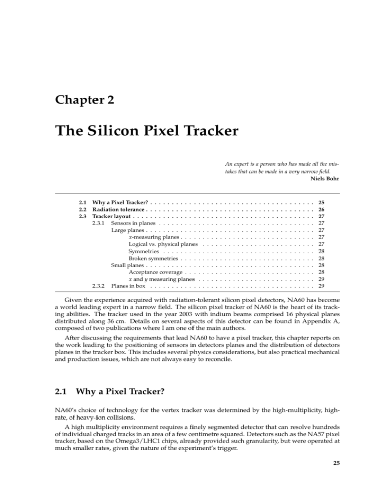
Chapter 2 The Silicon Pixel Tracker An expert is a person who has made all the mistakes that can be made in a very narrow field. Niels Bohr 2.1 2.2 2.3 Why a Pixel Tracker? . . . . . . . . . . . . Radiation tolerance . . . . . . . . . . . . . Tracker layout . . . . . . . . . . . . . . . . 2.3.1 Sensors in planes . . . . . . . . . . Large planes . . . . . . . . . . . . . x-measuring planes . . . . . Logical vs. physical planes Symmetries . . . . . . . . . Broken symmetries . . . . . Small planes . . . . . . . . . . . . . Acceptance coverage . . . . x and y measuring planes . 2.3.2 Planes in box . . . . . . . . . . . . . . . . . . . . . . . . . . . . . . . . . . . . . . . . . . . . . . . . . . . . . . . . . . . . . . . . . . . . . . . . . . . . . . . . . . . . . . . . . . . . . . . . . . . . . . . . . . . . . . . . . . . . . . . . . . . . . . . . . . . . . . . . . . . . . . . . . . . . . . . . . . . . . . . . . . . . . . . . . . . . . . . . . . . . . . . . . . . . . . . . . . . . . . . . . . . . . . . . . . . . . . . . . . . . . . . . . . . . . . . . . . . . . . . . . . . . . . . . . . . . . . . . . . . . . . . . . . . . . . . . . . . . . . . . . . . . . . . . . . . . . . . . . . . . . . . . . . . . . . . . . . . . . . . . . . . . . . . . . . . . . . . . . . . . . . . . . . . . . . 25 26 27 27 27 27 27 28 28 28 28 29 29 Given the experience acquired with radiation-tolerant silicon pixel detectors, NA60 has become a world leading expert in a narrow field. The silicon pixel tracker of NA60 is the heart of its tracking abilities. The tracker used in the year 2003 with indium beams comprised 16 physical planes distributed along 36 cm. Details on several aspects of this detector can be found in Appendix A, composed of two publications where I am one of the main authors. After discussing the requirements that lead NA60 to have a pixel tracker, this chapter reports on the work leading to the positioning of sensors in detectors planes and the distribution of detectors planes in the tracker box. This includes several physics considerations, but also practical mechanical and production issues, which are not always easy to reconcile. 2.1 Why a Pixel Tracker? NA60’s choice of technology for the vertex tracker was determined by the high-multiplicity, highrate, of heavy-ion collisions. A high multiplicity environment requires a finely segmented detector that can resolve hundreds of individual charged tracks in an area of a few centimetre squared. Detectors such as the NA57 pixel tracker, based on the Omega3/LHC1 chips, already provided such granularity, but were operated at much smaller rates, given the nature of the experiment’s trigger. 25 26 The Silicon Pixel Tracker Fluence [1 MeV neq cm-2] x1010 5000 Plane 0 Plane 15 4000 3000 2000 1000 Figure 2.1 Simulation of the integrated non-ionising energy loss for the 2003 In-In run. 2.2 0 0.4 0.6 0.8 1 1.2 1.4 Radial distance from beam axis [cm] Radiation tolerance The feasibility tests of the NA60 muon matching concept took place in the year 1998 with the pixel technology used in NA57. But even in p-Be collisions, where the multiplicity of produced particles is quite low, the detectors used were heavily deteriorated after a few days of operation. In fact, it was not the sensing elements themselves that stopped working, but rather the associated readout electronics. The conventional electronics used stopped working after having been exposed to a few tens of krad [1]. Thus a tracker able to operate for a full heavy-ion run had to wait for the development of readout electronics tolerant to radiation. Profiting from the LHC developments, NA60 used ALICE1LHCB readout chips, whose radiation tolerance, in excess of 10 Mrad, was found appropriate for NA60’s needs. This increased tolerance is achieved by using a thinner gate oxide (reducing the effect of charge build-up at the oxide surface) and the use of enclosed geometries (which restrict possible leakage current paths) [2]. The ALICE1LHCB readout chip has a matrix of 32 × 256 pixel cells of 425×50 µm2 area. Each pixel cell is equipped with a discriminator and digital logic operated at 10 MHz. Several ALICE1LHCB pixel readout chips share the readout bus, controlled by the Pilot chip, which sits outside of the magnet. Readout proceeds serially chip-by-chip whereas in each chip the 32 columns are read out in parallel, row-by-row. Given the clock speed, this means that eight chips in a bus are read out in not less than 8 × 256 × 100 ns, or 206.4 µs. This value was the limiting factor in the NA60 DAQ live-time, since all other detectors had a faster readout. Having the ionising energy-loss damage to the readout electronics under control, the main concern of NA60 became the non-ionising energy-loss damage to the silicon sensors. A simulation of the dose integrated for 5 weeks in the 2003 indium run is illustrated in Figure 2.1 for the first plane (plane 0) and last plane (plane 15). It shows that pixels closest to the beam line were exposed to roughly 1013 1 MeV neq cm−2 per week of running. Furthermore one can see that the radiation field is such that the dose drops by an order of magnitude from the inner to the outer regions. The tracker could be operated for the full extent of the 5-week indium 2003 run. We have observed radiation-induced phenomena, such as type-inversion of the sensor bulk and rising leakage current [3]. Such phenomena were expected and understood and all planes were subsequently reused in the proton run of 2004. 26 2.3 Tracker layout 2.3 27 Tracker layout Once the final magnetic field for the vertex tracker was known, we had to decide where to position each individual detector assembly inside the tracking volume provided. We have conducted extensive simulation using as figure-of-merit the coverage for single muons within the acceptance of the muon spectrometer. 2.3.1 Sensors in planes The first partitioning of detector assemblies is to group them into planes that share the same z coordinate. Ideally each plane could profit from having a different sensor layout, but in order to reduce the material budget and ensure the feasibility of the planes’ production, compromises are needed. By studying the acceptance of the NA60 trigger system and muon spectrometer, we have mapped as a function of z, which areas need to be covered in order to maximise the probability that a muon reconstructed in the muon spectrometer will have its corresponding vertex track is reconstructed in the pixel tracker. Taking into account this cone-shaped volume, composed by the sum of many cones with apexes in the subtargets, we immediately understood that planes were needed in two flavors: • Small planes properly cover the angular acceptance closest to the targets, while • Large planes are needed at larger z values, where muons from triggered events are spread over a wider transverse area. Large planes The layout for the 8-chip hybrids and the corresponding tracker set-up has been modified with respect to what was described in the experiment’s proposal [4]. Changes were motivated by the longer tracking distance allowed by the PT7 magnetic field and by the careful analysis of the bi-dimensional hit maps of muons reconstructed in the muon spectrometer after all online and offline cuts. In particular, there is a sizeable acceptance gap on the Jura side, around the y = 0 plane. This can be appreciated in Figure 2.2, where we overlay the final geometry for logical large planes to the density of muons in the transverse plane. Logical planes are composed of two physical planes, where the sensor assemblies are arranged as depicted in Figure 2.3. Contrary to what happened with the TC8 dipole magnet used in the proposal’s set-up and which had a vertical gap, the vertical field lines of the PT7 dipole magnet do not smear out those acceptance holes. x-measuring planes Measuring the kinematics of the muons dependens strongly on the matching of the detector geometry to the vertexing magnetic field, in our case a dipole field in the y direction. This means that particles are deflected in the xz projection, while following straight lines in the yz projection. Given the rectangular nature of the pixel cells, the planes can better measure the x or the y coordinate, depending on the orientation of the 50 µm side. Since the deflection takes place in the xz plane, it is crucial for the momentum resolution that the lever arm for the measurement of the x coordinate is largest. This leads to the logical conclusion that the large planes should all be of the x-measuring type. Logical vs. physical planes Large planes need 16 pixel assemblies to cover the whole angular acceptance. It is highly non trivial to pack so many assemblies together on a single hybrid, so it was decided to split each large plane into two physical units with half the detector assemblies and placed close to each other. Besides simplifying the cooling of the detector, this configuration has the further advantage of minimising the dead areas between the assemblies. This effect can be seen in Figure 2.2, where the depicted readout chips overlap, since their area is larger than the sensor’s active surface. However, this choice comes at the price of increasing the material budget of a futher support hybrid and of cooling structure. 27 The Silicon Pixel Tracker Y [cm] 28 X [cm] Figure 2.2 The logical 16-chip planes maximise the coverage of the acceptance of the muon spectrometer. The “Jura” side is on the right hand side of the plot. Figure 2.3 Arrangement of detector assemblies within an 8-chip pixel detector hybrid: two identical hybrids are combined in an upside-down geometry to form one logical 16-chip plane (illustrated in Figure 2.2). Symmetries Each pixel plane is composed of a number of elements that need to be designed, produced and assembled. Minimising the number of different elements needed saves times, reduces costs and optimises the testing and quality assurance procedures. For the large planes, the physical layout of the pixel assemblies is such that superimposing a plane with a plane flipped about the x axis will cover the full acceptance area. This entails that all physical large planes are identical and that half of them faces the beam, while the other half faces the hadron absorber, as depicted in Figure 2.4. Broken symmetries A last note on the design of the large planes concerns the asymmetry in the y position of the chips farthest away from the beam axis in the “Jura” direction (right hand side of Figures 2.2 and 2.3). This happens because the dimuon trigger has a blind zone, so-called “key-hole”. Though not part of the original design of NA10, this dead area demonstrates the spirit of experimental physics in its crudest form: NA10 used high intensity π − beams; since pions decay into muons, it was discovered soon after starting the experiment that there was a large amount of muons entering the spectrometer and flooding sextants 4 and 5, on the Jura side. This was promptly solved by cutting the scintillator slabs in sextants 4 and 5 of R3. This “key-hole” can be easily noticed in the asymmetry present in the muon cloud of reconstructed events, on the Jura side, as shown in Figure 2.2. Small planes The small pixel planes carry only 4 silicon pixel detector assemblies and three (of the 8) small planes have the small pixel side aligned with the y direction. Acceptance coverage Small planes have their chips tightly packed against each other in a fan-like structure. Unfortunately, a considerable area between adjacent assemblies is not sensitive. In order to minimise this, we have designed the small planes such that flipping a plane around the x axis yields a plane which covers the dead area of the unflipped plane. Flipping planes also helps packing of planes in the box, as discussed further below. 28 2.3 Tracker layout Small plane Flipped z [cm] Coverage [%] 29 x √ y x x √ y √ x y x 6.7 90.3 8.2 95.2 10.0 95.5 11.1 93.2 12.6 89.5 14.7 83.6 16.2 76.1 21.2 50.8 X √ X X √ X X √ X X √ X 17.6 51.7 19.7 52.0 22.2 51.6 24.3 51.5 26.0 50.5 28.0 49.6 30.1 45.4 33.0 43.7 Large plane Flipped z [cm] Coverage [%] Table 2.1 Layout of the pixel tracker used in the 2003 indium run, inside the PT7 magnet. Figure 2.4 Arrangement of the 16 detector planes (8× 4-chip + 8× 8-chip) of the NA60 silicon pixel tracker. The tracker is after the target system (left) and before the hadron absorber tip (right), between the PT7 magnet shims. x and y measuring planes The small planes were designed such that a single hybrid structure could be used to make x and y planes. The difference lies in a 90 degree rotation of the hybrid in the supporting PCB. Consequently, two different supporting PCB designs were needed. 2.3.2 Planes in box Pixel planes are complicated assemblies of detectors, electronics, passive components, connectors, mechanical elements and cooling structures. All these factors need to be kept in mind when placing the planes along the z direction inside the tracker box. Small planes are stacked in order to be as closely packed as possible, while large planes are laid more loosely, each physical pair centred around its optimal position. The arrangement of the detector planes in the full tracker is detailed in Table 2.1 and illustrated in Figure 2.4. The last line in Table 2.1 gives the fraction of single muons (from J/ψ decays) reconstructed in the Muon Spectrometer which will be detected in the geometrical acceptance of each of the 16 physical planes. The figure-of-merit in the optimisation of the plane distribution along the beam axis was given by a requirement inspired by the tracking algorithm: a muon should leave hits in at least one y plane, two small x planes and two large x planes. For the setup detailed in Table 2.1 and depicted in Figure 2.4, this criterion was fulfilled by 92.5% of the single muons reconstructed in the muon 29 30 The Silicon Pixel Tracker spectrometer and resulting from decays of J/ψ mesons produced at z = 0. When optimising the geometry of the vertex tracker, we have only taken into account the muons used in the traditional physics analyses of NA38 and NA50. For instance, events with muons whose reconstructed trajectories touch the ACM magnet’s iron sectors (18 degrees per sextant in φ) are rejected offline. Another “dead area” of the Muon Spectrometer is the fiducial volume at the centre of the wire chambers; muons going through that area cannot be tracked. These cuts are responsible for the loss of 27% and 9%, respectively, of single muons from J/ψ decays that reach the muon spectrometer acceptance. Consequently, the reference taken when optimizing the vertex tracker were single muons passing these cuts. We have not considered in this optimisation the preferences of non-dimuon physics analyses. For instance, the analysis of elliptical flow, which uses tracks measured in the target region, would benefit from a more symmetric azimuthal coverage of the acceptance by the geometry of the silicon pixel planes. It is worth mentioning that, with respect to the set-up used in the physics performance simulations made for the proposal, the increase in material budget due to the thicker readout chips is largely compensated by the thinner substrates, in particular in the planes closer to the targets, the most important for the track offset resolution. Bibliography [1] R. Arnaldi et al. NA60 Letter of Intent. May 1999. CERN/SPSC 1999-015 and SPSC/M 679. 26 [2] W. Snoeys et al. Pixel readout chips in deep submicron CMOS for ALICE and LHCb tolerant to 10-Mrad and beyond. Nucl. Instrum. Meth., A466:366–375, 2001. 26 [3] M. Keil et al. Studies of radiation effects in the NA60 silicon pixel detectors. Nucl. Instrum. Meth., A546:448–456, 2005. 26 [4] R. Arnaldi et al. NA60 Proposal. March 2000. CERN/SPSC 2000-010 and SPSC/P 316. 27 30
