ARTICLES
PUBLISHED ONLINE: 31 JANUARY 2010 | DOI: 10.1038/NPHYS1513
Static control logic for microfluidic devices using
pressure-gain valves
James A. Weaver1 *, Jessica Melin2 , Don Stark1 , Stephen R. Quake2 and Mark A. Horowitz1
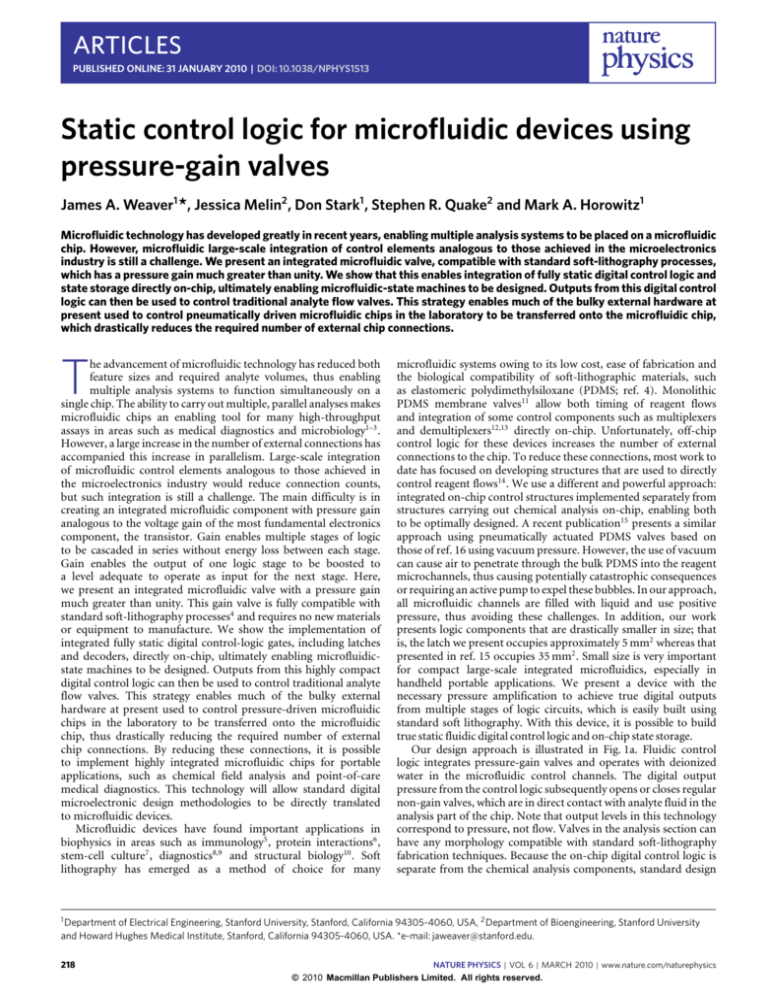
Microfluidic technology has developed greatly in recent years, enabling multiple analysis systems to be placed on a microfluidic
chip. However, microfluidic large-scale integration of control elements analogous to those achieved in the microelectronics
industry is still a challenge. We present an integrated microfluidic valve, compatible with standard soft-lithography processes,
which has a pressure gain much greater than unity. We show that this enables integration of fully static digital control logic and
state storage directly on-chip, ultimately enabling microfluidic-state machines to be designed. Outputs from this digital control
logic can then be used to control traditional analyte flow valves. This strategy enables much of the bulky external hardware at
present used to control pneumatically driven microfluidic chips in the laboratory to be transferred onto the microfluidic chip,
which drastically reduces the required number of external chip connections.
T
he advancement of microfluidic technology has reduced both
feature sizes and required analyte volumes, thus enabling
multiple analysis systems to function simultaneously on a
single chip. The ability to carry out multiple, parallel analyses makes
microfluidic chips an enabling tool for many high-throughput
assays in areas such as medical diagnostics and microbiology1–3 .
However, a large increase in the number of external connections has
accompanied this increase in parallelism. Large-scale integration
of microfluidic control elements analogous to those achieved in
the microelectronics industry would reduce connection counts,
but such integration is still a challenge. The main difficulty is in
creating an integrated microfluidic component with pressure gain
analogous to the voltage gain of the most fundamental electronics
component, the transistor. Gain enables multiple stages of logic
to be cascaded in series without energy loss between each stage.
Gain enables the output of one logic stage to be boosted to
a level adequate to operate as input for the next stage. Here,
we present an integrated microfluidic valve with a pressure gain
much greater than unity. This gain valve is fully compatible with
standard soft-lithography processes4 and requires no new materials
or equipment to manufacture. We show the implementation of
integrated fully static digital control-logic gates, including latches
and decoders, directly on-chip, ultimately enabling microfluidicstate machines to be designed. Outputs from this highly compact
digital control logic can then be used to control traditional analyte
flow valves. This strategy enables much of the bulky external
hardware at present used to control pressure-driven microfluidic
chips in the laboratory to be transferred onto the microfluidic
chip, thus drastically reducing the required number of external
chip connections. By reducing these connections, it is possible
to implement highly integrated microfluidic chips for portable
applications, such as chemical field analysis and point-of-care
medical diagnostics. This technology will allow standard digital
microelectronic design methodologies to be directly translated
to microfluidic devices.
Microfluidic devices have found important applications in
biophysics in areas such as immunology5 , protein interactions6 ,
stem-cell culture7 , diagnostics8,9 and structural biology10 . Soft
lithography has emerged as a method of choice for many
microfluidic systems owing to its low cost, ease of fabrication and
the biological compatibility of soft-lithographic materials, such
as elastomeric polydimethylsiloxane (PDMS; ref. 4). Monolithic
PDMS membrane valves11 allow both timing of reagent flows
and integration of some control components such as multiplexers
and demultiplexers12,13 directly on-chip. Unfortunately, off-chip
control logic for these devices increases the number of external
connections to the chip. To reduce these connections, most work to
date has focused on developing structures that are used to directly
control reagent flows14 . We use a different and powerful approach:
integrated on-chip control structures implemented separately from
structures carrying out chemical analysis on-chip, enabling both
to be optimally designed. A recent publication15 presents a similar
approach using pneumatically actuated PDMS valves based on
those of ref. 16 using vacuum pressure. However, the use of vacuum
can cause air to penetrate through the bulk PDMS into the reagent
microchannels, thus causing potentially catastrophic consequences
or requiring an active pump to expel these bubbles. In our approach,
all microfluidic channels are filled with liquid and use positive
pressure, thus avoiding these challenges. In addition, our work
presents logic components that are drastically smaller in size; that
is, the latch we present occupies approximately 5 mm2 whereas that
presented in ref. 15 occupies 35 mm2 . Small size is very important
for compact large-scale integrated microfluidics, especially in
handheld portable applications. We present a device with the
necessary pressure amplification to achieve true digital outputs
from multiple stages of logic circuits, which is easily built using
standard soft lithography. With this device, it is possible to build
true static fluidic digital control logic and on-chip state storage.
Our design approach is illustrated in Fig. 1a. Fluidic control
logic integrates pressure-gain valves and operates with deionized
water in the microfluidic control channels. The digital output
pressure from the control logic subsequently opens or closes regular
non-gain valves, which are in direct contact with analyte fluid in the
analysis part of the chip. Note that output levels in this technology
correspond to pressure, not flow. Valves in the analysis section can
have any morphology compatible with standard soft-lithography
fabrication techniques. Because the on-chip digital control logic is
separate from the chemical analysis components, standard design
1 Department
of Electrical Engineering, Stanford University, Stanford, California 94305-4060, USA, 2 Department of Bioengineering, Stanford University
and Howard Hughes Medical Institute, Stanford, California 94305-4060, USA. *e-mail: jaweaver@stanford.edu.
218
NATURE PHYSICS | VOL 6 | MARCH 2010 | www.nature.com/naturephysics
© 2010 Macmillan Publishers Limited. All rights reserved.
NATURE PHYSICS DOI: 10.1038/NPHYS1513
a
ARTICLES
On-chip
bio/chem-analysis system
On-chip
fluidic control logic
Pressurized DI water
Reagent
control
valve
Latch
Logic
Valves used have
Valves used have
pressure gain < 1
pressure gain >> 1
b
External
world
Microfluidic chip
Microfluidic bio/chem-analysis system
(with non-gain valves
in contact with analyte fluids)
Transfer output
to individual
control lines
1
Off-chip
serial control input
11010...0100
1
0
1
0
0
1
0 00
0
1
0
Fluidic state
register
Parallel
transfer
1
1
0
1
0
0
Fluidic shift
register
Shifting direction
Figure 1 | Microfluidic control-logic scheme. a, Schematic of the control-logic fundamental approach. On-chip control blocks are distinct from on-chip
analyte flow channels. The control blocks contain fully static digital fluidic logic and state storage realized by gain valves. Deionized water is used as the
working fluid. The output of the control-logic block connects to control channels in the bio/chem-analysis area of the chip. These control channels directly
control non-gain valves, which are in contact with the analyte fluid. b, The number of off-chip control lines can be reduced by serially inputting new control
states, using a fluidic shift register comprised of a number of serially connected latches. Here, binary inputs ‘0’ and ‘1’ correspond to low and high pressure,
respectively. The shift-register contents are then loaded in parallel into the fluidic register, where the outputs are decoded to control the microfluidic
bio/chem-analysis system. With this approach, a small number of (for example, five) input lines can control an arbitrarily large number of on-chip analyte
flow control lines.
tools may be borrowed from the microelectronics industry to design
microfluidic control circuits. Figure 1b illustrates the power of this
design strategy. A digital control block addresses the common
problem of an unmanageably large number of input–output chip
connections required for high-throughput chips by drastically
reducing this number. The control-logic block consists of (1) a shift
register, which accepts external control input serially (in a bit-by-bit
manner), and (2) a state register, which accepts and holds the output
of the shift register in a parallel manner (all bits at once). Bit states
‘0’ and ‘1’ correspond to low or high pressures, respectively. The
n-bit shift register consists of n serially connected digital latches, and
the n-bit state register of n parallel connected latches, where a latch
is a single-bit digital state-storage component (see Supplementary
Fig. S3). Only five inputs are required (control data input, two load
inputs, which trigger the loading of control data inputs, supply
pressure and ambient ‘ground’ pressure) to produce an arbitrary
number of defined control-logic outputs.
To construct fluidic control-logic devices, a valve with pressure
gain is needed; a control ‘signal’ of lower pressure must be able to
modulate fluid flow at a higher pressure. Numerous approaches to
creating such valves and microfluidic logic have been previously
reported. These include silicon valves17,18 and glass–elastomer
valves16,19,20 . The latter valves are large, occupying approximately
1 mm2 of area. Glass–elastomer valves can be used to create a
form of pulse-mode digital logic, and complex integrated logic
functions have been demonstrated using this approach21 . Pulsemode logic, however, is not an ideal logic family owing to its
complex timing constraints. Unlike static logic, where a signal
corresponds to a statically held pressure, signals in pulse-mode logic
are pressure pulses. In designing pulse-mode logic, propagation
delays and pulse width must be carefully considered to maintain
the timing coherence required for proper operation. Achieving
this balance can be difficult, and few design tools are available.
Digital state storage has been successfully demonstrated using
glass–elastomer valves to create dynamic latches16 and by using
non-Newtonian working fluids22 . Dynamic latches, however, must
be periodically refreshed to avoid data loss, and the behaviour of
non-Newtonian fluids can be complex. We address these issues with
a pressure-gain valve implemented entirely in standard planar soft
lithography that with required bonding area occupies 0.28 mm2
and enables fully static control-logic gates and latches to be
integrated on-chip.
NATURE PHYSICS | VOL 6 | MARCH 2010 | www.nature.com/naturephysics
© 2010 Macmillan Publishers Limited. All rights reserved.
219
NATURE PHYSICS DOI: 10.1038/NPHYS1513
ARTICLES
a
Source layer
Source
Exhaust layer
Membrane layer
Exhaust
Control layer
Disc
Control
Rigid disk
Orifice
b
Source layer
Flow
Exhaust layer
Membrane layer
Flow
Control layer
Figure 2 | Top and cross-sectional views of the gain-valve design. The gain valve consists of four PDMS layers: control layer; membrane layer containing
the rigid SU-8 disc, which enables force summation; exhaust layer; source layer. a, The valve closed. Pressure in the control line has forced the membrane
layer into contact with the exhaust layer, sealing off the orifice and stopping flow through the valve. Force summation occurs over the rigid disc, giving
pressure gain. b, The valve open. Low pressure in the control line enables the membrane to relax, opening the valve. The red arrow shows the direction of
fluid flow through the valve. The scale bars in the photographs are 300 µm long.
a
Opening threshold curve
200
175
100
Pressure (kPa)
PS (kPa)
120
Gain = 3
150
125
100
75
50
25
0
AND gate output pulse
b
25
50
75
60
40
20
Gain = 15
0
80
0
100 125 150 175 200
0
5
10
PC (kPa)
c
15
Time (s)
20
25
30
Latch operation
140
120
Pressure (kPa)
100
80
D
60
LD
40
/LD
Q out
20
0
0
0.5
1.0
1.5
2.0
2.5
3.0
Time (min)
3.5
4.0
4.5
5.0
Figure 3 | Performance graphs. a, Opening threshold pressure of 10 gain valves. The source line pressure, which is the pressure across the valve, is plotted
against the control pressure at which the valve just opens. The dashed line indicates a pressure gain of unity. The valves have an initial incremental gain of
approximately 15, which decreases to 3 at source pressures above 100 kPa. b, Low-to-high and high-to-low transitions measured at the output of an AND
gate showing exponential behaviour. The low-to-high time delay (measured at 50%) is 500 ms, and the high-to-low time delay is 50 ms at 50% threshold.
c, Measured pressure waveforms for a static latch. With the LD input high and the LD input (labelled /LD in the figure) low, the Q output (blue) follows the
D input (red). With the LD input low and the LD input high, the Q output remains latched high, dropping only when LD goes low.
220
NATURE PHYSICS | VOL 6 | MARCH 2010 | www.nature.com/naturephysics
© 2010 Macmillan Publishers Limited. All rights reserved.
NATURE PHYSICS DOI: 10.1038/NPHYS1513
a
ARTICLES
Control-logic area of chip
Logic output
Exhaust (ambient)
Pressure supply
Bio/chem-analysis area of chip
Analysis area Analyte
input
control input
Analyte
output
Source layer
Plow
Exhaust layer
Plow
Membrane layer
Plow
Plow
Control input Gain valve
b
Non-gain valve
Rigid disc
Control-logic area of chip
Logic output
Exhaust (ambient)
Pressure supply
Control layer
Bio/chem-analysis area of chip
Analysis area
control input Analyte
input
Analyte
output
Phigh
Phigh
Phigh
Control input
Gain valve
Non-gain valve
Figure 4 | Interconnection of on-chip control logic to analyte control valves. The control logic (inside the green box) uses deionized water as a working
fluid and incorporates the gain valve. The control-logic output is in the form of high–low pressures. This control-logic output connects to the control inputs
of non-gain membrane valves controlling analyte flows in the bio/chem-analysis area of the chip (inside the red box). The control-logic working fluid and
the reagent flows never mix. a, When the control input pressure is low (Plow ), the gain valve is open and the supply pressure is exhausted to ambient. The
output pressure from the control-logic block is low (Plow ). b, When the control input is high (Phigh ), the gain valve is closed and the output pressure from
the control block essentially becomes the supply pressure (Phigh ), thus closing the non-gain valve.
The greatest design challenge in constructing a valve with
pressure gain is the highly elastic nature of elastomeric materials
such as PDMS. When subjected to a force, all materials show
deformation and this is characterized by Young’s modulus, E
(refs 23, 24). Elastomers have very low E (for example, 400–800 kPa
for PDMS) and show large deformations when subjected to modest
force. This makes it difficult to build structures with the mechanical
advantage needed for pressure gain greater than unity. However,
this can be achieved by integration of a stiff material that is compatible with multilayer soft-lithography fabrication techniques. Some
valves with integrated stiff materials have been previously presented,
including a membrane valve with a steel disc embedded in PDMS
to realize a magnetically driven pump25 , a MEMS-based iron–nickel
membrane26 , and a parylene–silicon-based valve27 . However, the
valve of ref. 25 is fairly large: the embedded steel discs are 5 mm
in diameter, and the valves of refs 26 and 27, although compact,
require specialized manufacturing techniques and materials not
compatible with planar soft lithography. Our valve, shown in
Fig. 2, consists of four layers and is fully compatible with standard
soft-lithography fabrication processes: (1) source layer, (2) disc
layer, which incorporates a rigid disc made from SU-8, (3) exhaust
layer and (4) control layer (see Supplementary Information for fabrication details and valve dimensions). When pressure is applied to
the control port, the disc layer is driven into the exhaust layer until
they are in contact, thus sealing off the valve orifice and stopping
fluid flow through the gain valve (Fig. 2a). With no pressure in the
control port, the working fluid flows from the source line through
the valve orifice to the exhaust port (Fig. 2b). For switching applications, the exhaust port is maintained at a low pressure relative to the
source line. With the valve closed, the control pressure acts over the
entire bottom side of the disc layer, whereas the source pressure acts
only over the area of the orifice. The rigid disc (E ∼ 1 GPa) deforms
minimally and enables force summation across its surfaces. Thus, in
the closed state, the upper bound on the incremental pressure gain
is set by the ratio of the disc to orifice diameters:
Psource
Ddisc 2
AP =
=
(1)
Pcontrol
Dorifice
In our design, the disc diameter is 140 µm, and the orifice diameter
is 30 µm, which gives a pressure-gain upper bound of 22. In addition
to pressure gain, the valve also has a pressure threshold. This is the
control pressure required to drive the disc layer into contact with the
exhaust port ceiling at zero source line pressure. Using the design
dimensions (Supplementary Fig. S1) and a value of 500 kPa for the
shear modulus of PDMS, the threshold pressure is 34 kPa using
finite-element simulation.
Figure 3a shows the measured opening threshold pressures for
a representative sample of ten gain valves; all showed openingpressure gains greater than unity. The source line pressure, PS , is
plotted against the control port pressure, PC , at which a closed valve
just opens (exhaust line pressure is at ambient pressure). The slope
of the PS versus PC curve gave an average incremental gain of 15,
which is fairly close to the predicted upper bound (equation (1)).
As the source line pressure increases, the exhaust layer begins to
deform into the exhaust port, reducing the gain to 3 for source line
pressures above 100 kPa. This incremental gain of 3 was consistent
up to 172 kPa, the maximum PS value tested.
NATURE PHYSICS | VOL 6 | MARCH 2010 | www.nature.com/naturephysics
© 2010 Macmillan Publishers Limited. All rights reserved.
221
NATURE PHYSICS DOI: 10.1038/NPHYS1513
ARTICLES
a
b
Buffer
c
AND gate
PDD
PDD
PDD
IN1 • IN2
Out
IN
IN2
Reference
pressure
d
OR gate
IN1
Reference
pressure
IN2 = IN1 = 1
e
Inverter
Q
IN1 + IN2
IN1
Reference
pressure
IN2 = 1 IN1 = 0
Decoder
IN1
IN2
PDD
IN2
f
Latch
LD
D
LD
Y0
PDD
Y3
Y1
IN
Q
IN
Y2
LD
D
LD
Reference
pressure
Reference
pressure
IN = 0
IN1
IN2
Y0
D
IN2 = 0 IN1 = 1
IN2 = 0 IN1 = 1
IN = 1
LD
LD
IN2 = IN1 = 0
Y3
Y1
Q
Y2
IN2 = IN1 = 0
Figure 5 | Schematics and photomicrographs of implemented logic. The logic states ‘0’ and ‘1’ correspond to low and high pressure, respectively.
a, Simple buffer. The valve is in series with a fluidic resistor, and the output is at the valve’s source line. When the valve is closed, the output pressure is high
enough to close a similar gain valve; when the valve is open, the pressure drop across the resistor creates an output pressure low enough to open a similar
gain valve. Fluidic resistors are created in the exhaust layer because its thin cross-section allows for compact devices. b, Two-input AND gate. Flow paths
are shown for pressure inputs {IN1, IN2} = 11, 01 and 0. c, Two-input OR gate. Flow paths are shown for a similar sequence of input pressure levels as for the
AND gate. d, Simple inverter, showing flow paths for input pressure low and input pressure high. e, Static latch with dual-input load enable (see
Supplementary Fig. S3 and Movie M1). Lines unused in this implementation are covered by blue cross-hatching. f, Two-input to four-output decoder.
Correct operation of the decoder was verified with a supply pressure of 172 kPa. The two inputs were walked through all four possible combinations: 0, 01,
10 and 11 (where 1 = supply pressure). For each of these combinations, the correct output line was at supply pressure, whereas the remaining three outputs
were low (see Supplementary Movie M2). The scale bars in the photographs are 300 µm long.
Figure 4 demonstrates how the gain valve can be incorporated
in a total lab-on-chip device. Here a representative single gain valve
is shown, but in reality multiple connected gain valves are used to
create several control components contained in the control-logic
area of the chip. The output of the integrated gain valve is at its
source channel, which also forms the input to the control input of
the analysis area of the chip. The analysis area of the chip does not
contain any gain valves, only non-gain valves.
Constructing digital logic gates from the gain valves requires
a pressure signal from the output source flow that is sufficient
to control another valve. Analogous to resistor–transistor logic,
an early solid-state electronic logic family28 , we place a fluidic
resistor in series with the valve’s source line (see Fig. 5a). With
the orifice blocked, there is no flow through the valve, and the
pressure at the source line input to the valve rises to the supply
level, PS , which is sufficient to close the valve of a similarly
constructed buffer. When fluid can flow through the valve, the
pressure loss across the resistor drops the pressure at the source
line input below the threshold level of subsequent gates. Using
Poiseuille’s law, we calculated an open resistance for the valve of
1.31 × 10¹³ Pa s m−3 ; experimental measurement yielded a value of
1.41 × 10¹³ Pa s m−3 . The fluidic resistor pressure drop is set to be
at least 10 times that of the valve itself, resulting in an output
low pressure that is 10% of the source pressure. Figure 3b shows
the measured pressure output swing, and the output low level is
222
10% of the supply pressure. The interconnection tubing we use
has a measured resistance of 4.96 × 10¹¹ Pa s m−3 per millimetre
of length, so 28 mm of routing yields a resistance equal to the
resistance of the valve itself.
For AND gates (Fig. 5b), two valves are placed in parallel; high
pressure is required at both inputs to stop flow through the resistor
and enable the output to go high. Placing two valves in series
produces a fluidic OR gate (Fig. 5c). High pressure at either valve
stops the flow, giving the supply pressure of PDD at the source-line
end of the resistor. With OR gates, care must be taken to size the
fluidic resistor large enough such that the pressure drop across the
series valves still gives an output level low enough not to close valves
in succeeding logic stages. Inverters are designed with equal-size
fluidic resistors connected to both the source and exhaust (Fig. 5d).
The gate output is taken from the exhaust side of the lower resistor.
When the valve is blocked the output pressure is zero, and when the
valve is open the output pressure is half of the supply pressure PDD .
As shown in Fig. 3a, this degraded high pressure level is still high
enough to close a non-inverting buffer; as long as each inverter is
followed by a non-inverting stage, the gates operate correctly.
To verify gate operation, AND, OR and inverter gates were
fabricated (Fig. 5b–d) and tested. The non-inverting AND and
OR gates operate correctly with source pressures above 52 kPa,
and inverters operate correctly for source pressures above 117 kPa.
Because the output of an inverter is half the source pressure, these
NATURE PHYSICS | VOL 6 | MARCH 2010 | www.nature.com/naturephysics
© 2010 Macmillan Publishers Limited. All rights reserved.
NATURE PHYSICS DOI: 10.1038/NPHYS1513
ARTICLES
two results indicate that mixed inverting and non-inverting logic
must have a source pressure of at least 138 kPa to operate properly.
Graphs of source supply pressure versus transition thresholds are
shown in Supplementary Fig. S2. Lifetime and characterization
testing is ongoing, but gain valves in an AND gate operating
at 103 kPa have been cycled more than 10,000 times without
observable gain reduction or defect.
These gates (AND, OR, inverter) form a complete set of logic
functions29 . Any desired binary function can be implemented with
combinations of these gates, and their static nature ensures that a
correct result is obtained after a finite time delay. Figure 3b shows
the measured pressure-versus-time trace of a single AND gate; the
rise and fall delay times measured at a threshold of 50% of full
swing are 500 ms and 50 ms respectively, which is comparable to
timing of the technology presented in ref. 15. This delay is caused
by the displacement of the volume of the measurement apparatus
through the fluidic resistor for the rising transition and through the
open valve for the falling transition, and reflects their 10:1 resistance
ratio. The volume displacement of the measurement apparatus
was approximately six times the control-volume displacement of
a single valve. In real applications, the displacement volume and
the delay depend linearly on the number of input gates connected
to an output. However, because every gate generates a full swing
output, an arbitrary number of gates can be placed in series. Using
lithographically produced microvias30 to interconnect the source,
exhaust and control channels, we constructed a latch (Fig. 5e) and
a two-into-four binary decoder (Fig. 5f). Note that the technology
presented in ref. 15 also requires vias; however, these were realized
by a more labour-intensive procedure of hole punching using a
blunt-tipped syringe. Our latch is fully static; once loaded, it will
hold its state indefinitely, as shown by the measured latch output
pressure trace in Fig. 3c. The slightly increased low output level
results from the two valves in series in the OR gates used. Increasing
the pressure drop across the fluidic resistor (see Fig. 5e) will lower
this level. In Supplementary Fig. S3 and Movies M1,M2 a schematic
diagram of latch operation and movies of an operating latch and
two-to-four decoder are shown. Finally, it should be noted that ring
oscillators can easily be made by connecting an odd number of (for
example, five) inverters in series, providing on-chip timing sources.
Received 8 July 2009; accepted 17 December 2009;
published online 31 January 2010
References
1. Melin, J. & Quake, S. R. Microfluidic large-scale integration: The evolution of
design rules for biological automation. Annu. Rev. Biophys. Biomol. Struct. 36,
213–231 (2007).
2. Dittrich, P. S., Tachikawa, K. & Manz, A. Micro total analysis systems. Latest
advancements and trends. Anal. Chem. 78, 3887–3907 (2006).
3. Breslauer, D. N., Lee, P. J. & Lee, L. P. Microfluidics-based systems biology.
Mol. BioSyst. 2, 97–112 (2006).
4. Quake, S. R. & Scherer, A. From micro to nano fabrication with soft materials.
Science 290, 1536–1540 (2000).
5. Einav, S. et al. Discovery of a hepatitis C target and its pharmacological
inhibitors by microfluidic affinity analysis. Nature Biotech. 28,
1019–1027 (2008).
6. Maerkl, S. J. & Quake, S. R. A systems approach to measuring the binding
energy landscapes of transcription. Science 315, 233–237 (2007).
7. Gomez-Sjoberg, R., Leyrat, A. A., Pirone, D. M., Chen, C. S. & Quake, S. R.
Versatile, fully automated, microfluidic cell culture system. Anal. Chem. 79,
8557–8563 (2007).
8. Yager, P. et al. Microfluidic diagnostic technologies for global public health.
Nature 442, 412–418 (2006).
9. Myers, F. B. & Lee, L. P. Innovations in optical microfluidic technologies for
point-of-care diagnostics. Lab Chip 8, 2015–2031 (2008).
10. Anderson, M. J., Hansen, C. L. & Quake, S. R. Phase knowlege enables
rational screens for protein crystallization. Proc. Natl Acad. Sci. USA 103,
16746–16751 (2006).
11. Unger, M. A., Chou, H.-P., Thorsen, T., Axel, S. & Quake, S. R. Monolithic
microfabricated valves and pumps by multilayer soft lithography. Science 288,
113–116 (2000).
12. Thorsen, T., Maerkl, S. J. & Quake, S. R. Microfluidic large-scale integration.
Science 298, 580–584 (2002).
13. Liu, J., Hansen, C. & Quake, S. R. Solving the ‘word-to-chip’ interface problem.
Anal. Chem. 75, 4718–4723 (2003).
14. Leslie, D. C. et al. Frequency-specific flow control in microfluidic circuits with
passive elastomeric features. Nature Phys. 5, 231–235 (2009).
15. Rhee, M. & Burns, M. A. Microfluidic pneumatic logic circuits and digital
pneumatic microprocessors for integrated microfluidic systems. Lab Chip 9,
3131–3143 (2009).
16. Grover, W. H., Ivester, R. H. C., Jensen, E. C. & Mathies, R. A. Development
and multiplexed control of latching pneumatic valves using microfluidic logical
structures. Lab Chip 6, 623–631 (2006).
17. Quero, J. M., Lugue, A. & Franquelo, L. G. ISCAS Vol. 2, 588–591 (IEEE
Phoenix, 2002).
18. Takao, H., Ishida, M. & Sawada, K. A pneumatically actuated full in-channel
microvalve with MOSFET-like function in fluid channel networks. IEEE J.
Micromech. Syst. 11, 421–426 (2002).
19. Grover, W. H., Skelley, A. M., Liu, C. N., Lagally, E. T. & Mathies, R. A.
Monolithic membrane valves and diaphragm pumps for practical large-scale
integration into glass microfluidic devices. Sens. Actuat. B 89, 315–323 (2003).
20. Hua, Z. et al. A versatile microreactor platform featuring a chemical-resistant
microvalve array for addressable multiplex syntheses and assays.
J. Micromech. Microeng. 16, 1433–1443 (2006).
21. Jensen, E. C., Grover, W. H. & Mathies, R. A. Micropneumatic digital
logic structures for integrated microdevice computation and control.
IEEE J. Micromech. Syst. 16, 1378–1385 (2007).
22. Groisman, A., Enzelberger, M. & Quake, S. R. Microfluidic memory and
control devices. Science 300, 955–958 (2003).
23. Timoshenko, S. P. & Goodier, J. N. Theory of Elasticity 3rd edn, 8–10
(McGraw-Hill, 1970).
24. Riande, E., Diaz-Calleja, R., Prolongo, M., Masegosa, R. & Salom, C.
Polymer Viscoelasticity 196–237 (Dekker, 1999).
25. Haeberle, S., Schmitt, N., Zengerle, R. & Ducree, J. Centrifugo-magnetic pump
for gas-to-liquid sampling. Sens. Actuat. A 135, 28–33 (2007).
26. Luharuka, R., LeBlanc, S., Bintoro, J. S., Berthelot, Y. H. & Hesketh, P. J.
Simulated and experimental dynamic response characterization of an
electromagnetic microvalve. Sens. Actuat. A 143, 399–408 (2008).
27. Chen, P.-J., Rodger, D. C., Meng, E. M., Humayun, M. S. & Tai, Y.-C.
Surface-micromachined parylene dual valves for on-chip unpowered
microflow regulation. IEEE J. Micromech. Syst. 16, 223–231 (2007).
28. Shiva, S. G. Introduction to Logic Design 2nd edn, 84–85 (Dekker, 1998).
29. Shiva, S. G. Introduction to Logic Design 2nd edn, 502–503 (Dekker, 1998).
30. Kartalov, E. P., Walker, C., Taylor, C. R., Anderson, W. F. & Scherer, A.
Microfluidic vias enable nested bioarrays and autoregulatory devices in
Newtonian fluids. Proc. Natl Acad. Sci. USA 103, 12280–12284 (2006).
Acknowledgements
We would like to acknowledge NIH R01 HG02644 Quake, 03/05/04-04/30/09. This work
was funded by unrestricted funds from the Electrical Engineering Department of
Stanford University. Finally, one of the authors, S.R.Q., co-founded a microfluidics
company (Fluidigm).
Author contributions
M.A.H. and S.R.Q. contributed the initial idea of using on-chip static fluidic logic to
reduce chip connection counts for large analysis chips. J.A.W., J.M. and D.S. contributed
equally to gain-valve and logic development, experimental measurements and
manuscript preparation.
Additional information
The authors declare no competing financial interests. Supplementary information
accompanies this paper on www.nature.com/naturephysics. Reprints and permissions
information is available online at http://npg.nature.com/reprintsandpermissions.
Correspondence and requests for materials should be addressed to J.A.W.
NATURE PHYSICS | VOL 6 | MARCH 2010 | www.nature.com/naturephysics
© 2010 Macmillan Publishers Limited. All rights reserved.
223
