White Paper
Crossbar Resistive Memory:
The Future Technology for NAND Flash
By Hagop Nazarian, Vice President of Engineering and Co-Founder
Abstract
NAND Flash technology has been serving the storage memory applications market for several decades –
thus creating a dependency that has steadily increased due to its scaling technology. However, in recent
years, further scaling of this technology has shown profound limitations. Currently, it is widely accepted
that scaling below 25nm has significantly degraded performance and reliability, thus, resulting in significant
overhead complexity and computational power-demand from the system controller. System manufacturers
as well as NAND Flash manufactures have begun the quest for a new technological solution. The most
promising emerging technology is Resistive Memory. In this paper we will first provide an overview of NAND
technology and the promising attributes of Crossbar’s nonvolatile RRAM technology. We will also explain the
benefits offered by Crossbar’s technology, its characteristics and why it is the replacement technology for
next generation NAND Flash.
NAND Technology Overview
NAND Flash technology has the largest market share in the nonvolatile memory (NVM), serving as the
preferred mass storage media in applications such as solid state drives (SSD), removable media storage
devices (USB and SD cards used in cameras, video recorders, and music players), tablets, smart phones
and media players.
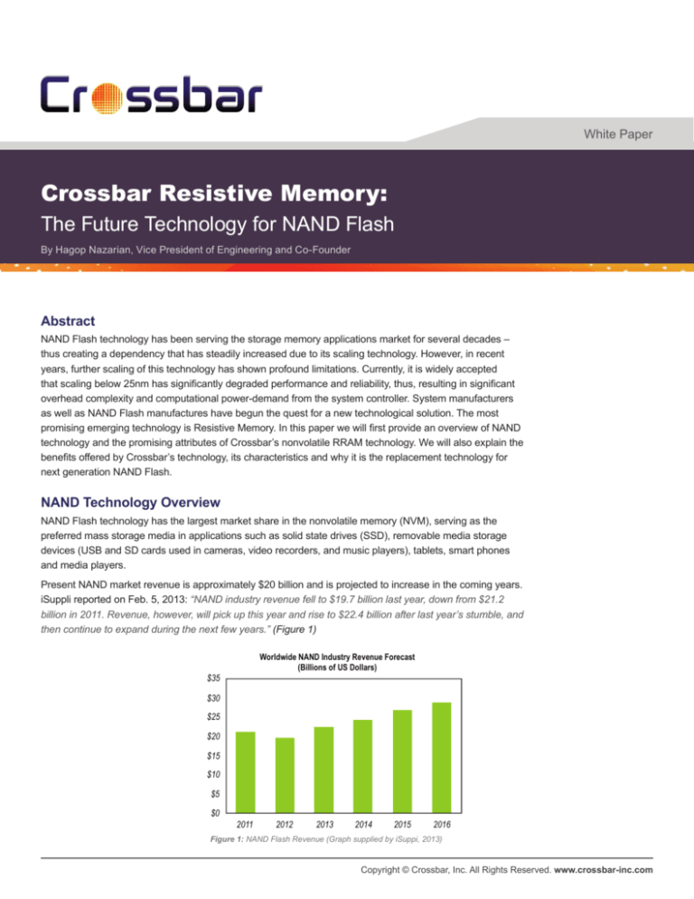
Present NAND market revenue is approximately $20 billion and is projected to increase in the coming years.
iSuppli reported on Feb. 5, 2013: “NAND industry revenue fell to $19.7 billion last year, down from $21.2
billion in 2011. Revenue, however, will pick up this year and rise to $22.4 billion after last year’s stumble, and
then continue to expand during the next few years.” (Figure 1)
Worldwide NAND Industry Revenue Forecast
(Billions of US Dollars)
$35
$30
$25
$20
$15
$10
$5
$0
2011
2012
2013
2014
2015
2016
Figure 1: NAND Flash Revenue (Graph supplied by iSuppi, 2013)
Source: IHS iSuppli Research, Janurary 2013
Copyright © Crossbar, Inc. All Rights Reserved. www.crossbar-inc.com
The Future Technology for NAND Flash
The NAND structure was introduced in 1987 by Dr. Fujio Masuoka from Toshiba. This structure uses a string
of EEPROM transistors connected in a series. Figure 2 shows an SEM cross section of a 90nm NAND
structure, and Figure 3 shows a schematic representation of the NAND structure with the corresponding
representative cross sections. The serial connection of the NAND array and the high efficiency array
structure provide excellent array efficiency and scaling properties up to the 25nm technology node.
NAND manufacturers, such as Samsung, Toshiba, and Micron, are already shipping 25nm and 20nm NAND
products. However, NAND technology scaling below 25nm has shown severe reliability and performance
degradation, which demands increased overhead and computational power from the NAND controller logic
and the host system.
Bit Line
Ground
Select
Transistor
Word
Line 0
Word
Line 1
Word
Line 2
Word
Line 3
Word
Line 4
Word
Line 5
Word
Line 6
Bit Line
Select
Transistor
Word
Line 7
Source Line
N
N
N
N
N
N
N
N
N
N
N
P
Figure 2: NAND Cross Section
Figure 3: A Schematic Representation of NAND
Industry Views on Current NAND Flash Technology
IEDM 2010 Presentation
During the IEDM 2010 Presentation, Micron/Intel presented a paper titled “25nm
64Gb MLC NAND Technology and Scaling Challenges,” in which several severe
scaling challenges facing NAND Flash were reviewed. According to Micron/Intel,
these challenges included the following:
Michael Yang
• Increase in floating gate to floating gate coupling ratio
created in the past two years. The creation and
Senior Principal Analyst, Memory and Storage, IHS
“Ninety percent of the data we store today was
• Increase in RTS noise
instant access of data has become an integral
• Reduction of the number of electrons in the floating
gate (30-50 electrons for 300mv-500mv VT separation)
dramatic growth for storage for the foreseeable
part of the modern experience, continuing to drive
future. However, the current storage medium,
• Increased impact of trapped electrons to change VT
planar NAND, is seeing challenges as it reaches
• Program noise due to random quantum
mechanical tunneling
the lower lithographies, pushing against physical
and engineering limits. The next generation nonvolatile memory, such as Crossbar’s RRAM, would
• System overhead (25bit ECC for 512B)
bypass those limits, and provide the performance
2011 Flash Summit
During the 2011 Flash Summit, SanDisk also presented the current scaling
implications of NAND technology by illustrating the growing gap between
application requirements and NAND performance and reliability degradation.
and capacity necessary to become the replacement
memory solution.”
Copyright © Crossbar, Inc. All Rights Reserved. www.crossbar-inc.com
The Future Technology for NAND Flash
The Best Candidate for NAND Flash Replacement
Scaling NAND technology adversely impacts the retention and cycling
characteristics of Flash NAND and the storage system. For example, scaling
from 72nm to 20nm has shown an increase of the raw bit error rate (BER)
from 1e-7 to 1e-2, and a decrease of cycling from 10,000 cycles to below
3,000 cycles.
Emerging storage applications, conversely, demand higher reliability and
endurance. Because of this, NAND manufacturers are realizing that present
planer NAND Flash technology has reached a limit that will not be able to serve
these applications. The widening gap between application requirements and
Flash technology has spurred industry professionals to look into new solutions to
resolve these issues.
RRAM-based disruptive technologies have been sited and chosen by major R&D
corporations as the best potential replacement for NAND Flash.
Greg Wong
At IEDM 2010, Sungjoo Hong from Hynix stated that “RRAM can be one of
the suitable candidates for a storage application due to its possibility of multistackable crosspoints.”
Founder, President and Principal Analyst,
Forward Insights
During the 2011 Flash Summit, SanDisk CTO Yoram Cedar presented this
message: “3D RRAM technology development shows the best promise for a
scalable post- NAND technology”.
developing a next generation memory technology
Again, at the 2013 ISSCC, Tz-Yi Liu from SanDisk presented “32Gbit RRAM
Memory Device in 24nm Technology,” where he stated that “RRAM has been
considered one of the potential technologies for the next generation nonvolatile
memory, given its fast access speed, high reliability, and multi-level capability.”
that will lead to significant improvements in
reliability, performance, low power operation
and scalability compared to existing non-volatile
memories. Forward Insights believes that RRAM,
including Crossbar’s approach, has the potential to
succeed NAND flash memory due to its scalability
and manufacturability. With the realization of a
working demo array, we are excited to see the
Crossbar 3D Resistive Memory Technology
future impact of this technology on a wide range of
Crossbar RRAM technology is based on filamentary nanoparticles while
using simple CMOS compatible materials. Each cell is located at the crossbar
junction of metal layers and it scales down to at minimum 5nm nodes. The cell
is manufactured at low temperatures and is built between interconnecting metal
layers as shown in Figure 4. Figure 5 shows a representative cross section of
Crossbar technology.
Figure 4: Crossbar RRAM Cell — The Crossbar cells are
sandwiched between interconnecting layers.
“For several years now, companies have focused on
applications from mobile and connected devices, to
storage and data centers.”
Figure 5: How it Works — In a switching media,
nanoparticles form a conduction path between the top
and bottom electrodes.
Copyright © Crossbar, Inc. All Rights Reserved. www.crossbar-inc.com
The Future Technology for NAND Flash
Crossbar Memory Characteristics
Stackable. A Crossbar cell is stackable, therefore, providing high density
3D arrays without occupying additional silicon area. This feature provides
a significant advantage in lowering the cost per gigabit. Plus, by improving
the array efficiency and die size compared to existing NAND technology, it
accommodates the trend toward smaller devices.
Figure 6 shows a representative cross section of the Crossbar cell array integrated
on top of the CMOS controller logic. Note that the area under the array is used
for building the CMOS circuits, which increases the array efficiency and results in
significant die size savings.
Sherry Garber,
Founding Partner, Convergent Semiconductors
“RRAM is widely considered the obvious leader
in the battle for a next generation memory and
Crossbar is the company most advanced, showing
a working demo that proves the manufacturability
of RRAM. This is a significant development
in the industry, as it provides a clear path to
commercialization of a new storage technology,
capable of changing the future landscape of
electronics innovation.”
Four Crossbar Memory Layers:
(4F2 /4 = 1F2)
Stacking enables true high
density
Repeating same step simplifies
memory process toolset
Two Metallization Layers :
Route signals from controller logic
to memory array
CMOS Controller Logic:
Tucked under memory array to
save die space
No large high voltage transistors
required
Figure 6: 4-Layer Crossbar Array — The representative cross section illustrates how the array is built on top of the CMOS.
Rectifying and Large Roff/Ron Ratio. The IV curve in Figure 7 shows several
distinctive properties of the Crossbar RRAM memory cell. Two of them, the large
Ion/ Ioff ratio (>1000) and the rectifying characteristic of the memory cell, are key
factors that will support products with large sensing margins, MLC operations,
and high density array constructions – all suitable for future high density market
segments.
Manufactured at Low Temperatures. Because the cell is manufactured at
low temperatures, it is compatible with CMOS and can be easily integrated into
existing systems.
Low Programming Current. Because it is dominated by electric fields, it
requires only a low programming current – current range of 1μA to 10μA per
programming cycle.
Low Voltage. Because it is not based on Joule heating phenomenon or high
current conduction, like other PCRAM and RRAM technologies, a typical
programming requires only approximately 3 volts.
Figure 7: 50nm x 50nm RRAM Cell IV — The curve
illustrates several distinctive properties of the Crossbar
RRAM memory cell.
Fast Switching Time. Because it is driven by electric fields, the switching time is
100ns or less per programming cycle.
Copyright © Crossbar, Inc. All Rights Reserved. www.crossbar-inc.com
The Future Technology for NAND Flash
Characteristics
NAND
Crossbar RRAM
Comments
Effective Cell Size (SLC)
5.44F2
4.28F2
RRAM provides better array efficiency and smaller
die size
Technology Scalability
Performance degradation
below 25nm
<5nm
Scales since it is nanoparticle-based memory
Stackable/MLC
MLC
Stackable MLC
RRAM provides smaller die size, CMOS circuits can
be built under the 3D RRAM array
Process Complexity
Complex FEOL Periphery
HV transistors do not
scale
Simpler BEOL compatible
with CMOS tech scaling
RRAM does not need ultra-high voltage transistors.
Easier to integrate with standard CMOS
technologies
Program Performance
7MB/sec
140MB/sec
RRAM performance is 20x faster
Page Erase / Byte Erase
Not Available
Not Required
RRAM significantly improves system performance
by not requiring Erase prior to Program
Byte Program
Not Available
Available
RRAM significantly improves system performance
Asynchronous (XIP) Read
.04MB/sec
17MB/sec
RRAM will provide faster NAND-like products
Program Energy/Cell
1360pJ/cell
64pJ/cell
RRAM improves programming performance and
power consumption
Endurance
3K cycles
1E6
RRAM improves memory system lifetime and
performance by eliminating wear-leveling due to
high endurance
Retention
1-3 years
20yr
RRAM provides significant improvement to system
lifetime and reliability due to better retention
Table 1: Key Attributes — The table compares the key attributes of NAND and Crossbar RRAM
Copyright © Crossbar, Inc. All Rights Reserved. www.crossbar-inc.com
The Future Technology for NAND Flash
Conclusion
Crossbar’s patented nonvolatile RRAM memory technology exhibits the physical
and electrical performance characteristics that are the key to driving the storage
system evolution without sacrificing performance and reliability.
With these breakthrough characteristics, Crossbar RRAM promises to provide
storage systems with high density, superior performance and superior reliability
and satisfy the needs of next generation devices.
RRAM’s Characteristics
• Simple cell structure
• CMOS compatible material
• Small cell structure ≤4F2
• Scalability to 5nm node
• Low program/erase current
≤2μA, high Roff/Ron ratio >1000
• 3D stackability
• High endurance
• Long retention
• Low power
• Multi-level
Jim Handy
Director, Objective Analysis
“The memory market is looking to new technologies
to take over once flash reaches its scaling limit.
Crossbar’s impressive progress in the development
of a manufacturable ReRAM gives a big boost to this
popular alternative memory.”
Alan Niebel
Founder and CEO, WebFeet Research
“To date, there has not been a viable 2D or 3D
NAND replacement technology. Storage Class
Memories like Crossbar’s RRAM have a chance of
capturing this elusive NAND replacement $40+ billion
prize. Crossbar’s working RRAM technology array
demonstrates significant commercialization progress.
Continuing on this trajectory they could lead the market
with a cost effective crosspoint, multi-layer (8) RRAM
ahead of the 3D NAND or their 3D RRAM competition.”
www.crossbar-inc.com
Headquarters:
3200 Patrick Henry Dr.
Suite 110
Santa Clara, CA 95054
Phone: (408) 884-0281
Email: info@crossbar-inc.com
Founded in 2010, Crossbar, a start-up based in Santa Clara, California, is the inventor of a new class of non-volatile RRAM memory technology.
Designed to usher in a new era of electronics innovation, Crossbar will deliver up to a terabyte (TB) of storage on a single-chip the size of a postage
stamp, with very low power, very high performance and compatibility with standard CMOS semiconductor manufacturing processes. As the exclusive
holder of resistive RAM (RRAM) patents from the University of Michigan, Crossbar has filed 100 unique patents, with 30 already issued, relating to
the development, commercialization and manufacturing of RRAM technology. Crossbar is backed by Artiman Ventures, Kleiner Perkins Caufield &
Byers and Northern Light Venture Capital. For more information, visit www.crossbar-inc.com.
Copyright 2013. All rights reserved. Crossbar, Inc., the Crossbar logo and certain other Crossbar trademarks and logos are trademarks and/or
registered trademarks of Crossbar, Inc.
0813
