A 1.35 GS/s, 10b, 175 mW Time-Interleaved AD Converter in 0.13
A 1.35 GS/s, 10b, 175 mW Time-Interleaved AD Converter in 0.13 µm CMOS
Simon M. Louwsma, Ed J.M. van Tuijl, Maarten Vertregt* and Bram Nauta
IC Design Group, CTIT Research Institute, University of Twente
Abstract
A time-interleaved ADC is presented with 16 channels, each consisting of two Successive Approximation (SA) ADCs in a pipeline configuration. Three techniques are presented to increase the speed of an SA-ADC. Single channel performance is 6.9 ENOB at an input frequency of 4 GHz.
Multi-channel performance is 7.7 ENOB at 1.35 GS/s with an
ERBW of 1 GHz and a FoM of 0.6 pJ/conversion-step.
Keywords: ADC, SAR, SA-ADC, time-interleaved, T/H.
Motivation
A trend in receiver design for digital-TV, satellite receivers and set-top boxes is the move towards software defined radios, where the embedded Analog-to-Digital Converter
(ADC) is moved closer to the antenna. Such ADCs require
8-10 bits of resolution for GHz range of signals and limited power consumption of a few hundred mWs.
Architecture
The Successive Approximation (SA) ADC architecture has a high power efficiency; it uses only 1 comparator, which makes it suitable for nanometer scale technologies. Its operation speed is however limited at high resolution: for an n -bit converter, n iterations are required.
By time-interleaving multiple ADCs the operation speed is increased by the interleaving factor [1,2]. A trade-off exists between this factor and the power required for a buffer driving the input load. Here a moderate interleaving factor of
16 is chosen based on the interleaved T/H presented in [3]. In this design an improved version is used which has more bandwidth, includes bootstrapping of the sampling switch for enhanced linearity and includes gain and offset calibration.
An interleaving factor of 16 still requires a high samplerate of the sub-ADCs. In this design three techniques are used to get a high sample-rate and good power efficiency:
(1) two SA-ADCs are combined in a pipeline configuration
(2) the single-sided overrange technique (3) look-ahead logic.
Sub-ADC architecture
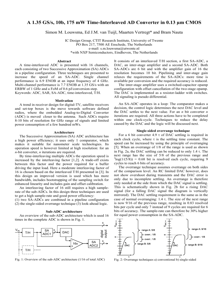
An overview of the sub-ADC architecture which is used 16 times in the complete ADC is shown in Fig. 1.
6
PO Box 217, 7500 AE Enschede, The Netherlands e-mail: s.m.louwsma@utwente.nl
*with NXP Semiconductors, Eindhoven, The Netherlands
It consists of an interleaved T/H section, a first SA-ADC, a
DAC, an inter-stage amplifier and a second SA-ADC. Both
SA-ADCs are 6 bit and with the amplifier gain of 16 the resolution becomes 10 bit. Pipelining and inter-stage gain relaxes the requirements of the SA-ADCs: more time is available per conversion and the required accuracy is reduced.
The inter-stage amplifier uses a switched-capacitor opamp configuration with offset cancellation of the two-stage opamp.
The DAC is implemented as a resistor-ladder with switches.
All signaling is pseudo differential.
An SA-ADC operates in a loop: The comparator makes a decision, the control logic determines the next DAC level and the DAC settles to the next value. For an n bit converter n iterations are required. All three actions have to be completed within one clock-cycle. Techniques to reduce the delay caused by the DAC and the logic will be discussed next.
Single-sided overrange technique
For a 6 bit converter 4.9 τ of DAC settling is required in each clock cycle, where τ is the settling time constant. The speed can be increased by using the principle of overranging
[5]. When an overrange of 1/8 of the range is used as shown in Fig. 2a, the DAC settling can be reduced to only 1.4 τ . The next range has the size of 5/8 of the previous range and
2 log(1/(5/8)) = 0.68 bit is resolved each cycle, requiring 9 cycles to reach 6 bits of accuracy.
The overrange technique assumes overrange on both sides of the comparison level. An RC limited DAC however, does not show overshoot during transients and the DAC error is only due to incomplete settling. An overrange is therefore only needed at the side from which the DAC signal is settling.
This is schematically shown in Fig. 2b for a rising DAC signal (for a falling DAC signal the diagram is vertically mirrored). The DAC settling requirement is the same as in the case of normal overranging: 1.4 τ . The size of the next range is now 9/16 of the previous range, resulting in 0.83 resolved bits per cycle and only 7 instead of 9 cycles are required for 6 bits of accuracy. The sample-rate can therefore be 30% higher for equal power consumption in the SA-ADC.
V
IN
T/H
SA
ADC1
6
DAC
-
+
16x
SA
ADC2
6
Fig. 1: Overview of the sub-ADC architecture (1/16 of total ADC) t t t t
Fig. 2: Overrange techniques a) conventional b) single-sided
Look ahead logic
To reduce the logic delay, the following technique is used:
After each comparator decision there are two possible DAC levels, which are calculated in advance. Once the decision is known, the right level only has to be picked.
This is implemented as follows: The control logic connects two outputs of the comparator via transmission-gates to the appropriate switches in the resistor-ladder DAC. The two comparator outputs are initially both zero and after a decision, only one of them becomes active high, immediately starting the DAC settling. Any logic gate-delay is avoided.
Calibration
Time-interleaved ADCs often require calibration of gain and offset [1,2] and sometimes of timing [1]. Here, calibration of channel gain and offset is used to correct for deviations caused by the use of small T/H buffers [3]. Comparator offset is calibrated to enable the use of small differential pairs to keep the load for the DAC small. We use a symmetrical design and a master clock [3,4] to get good timing alignment and to avoid complicated timing calibration.
Gain and offset calibrations are controlled digitally by modifying analog bias settings to correct for the cause of deviation. This way no part of the input window is sacrificed and high-speed power-hungry digital operations are avoided.
In this test-chip the calibration of the digital bias control registers is performed manually. In an actual implementation the calibration can be performed at start-up and only easy-togenerate DC test signals are needed.
The ADC is fabricated in 0.13 µm CMOS and a photograph of the chip is shown in Fig. 3. The active area is 1.6 mm 2 .
70
65
60
55
50
11
10
9
8
45
40
SFDR
-THD
SNR
SNDR
7
6
Col
35
0.1
1
Input frequency [GHz]
10
Fig. 4: Measurement result of a single channel
Compared to the single channel case, the performance is only slightly degraded, proving that the calibrations are accurate.
Static timing offsets between channels degrade the total timing error to 0.6 ps rms. This value is even slightly better than the best found in literature [1] where complicated timing calibration is used. At 2 GHz the SNDR is 6.5 ENOB and at
4 GHz the SNDR is 5.8 ENOB, limited by timing offsets between channels. The analog input bandwidth is estimated at
6 GHz. The T/H buffers use a supply of 1.6 V, while the rest uses 1.2 V. Total power consumption is 175 mW. The FoM calculated by power/(2 ENOB * min(f s
, 2*ERBW)) is 0.6 pJ per conversion-step. Note that the ERBW of 1 GHz is much larger than ½ f
S
and broadband signal handling capability is demonstrated through continued graceful degradation
(6 dB/octave) up to a record input frequency of 8 GHz.
65
10
60
55
9
50 8
Fig. 3: Photograph of the time-interleaved ADC
Measurement results
First, the measurement result of a single channel is discussed. During this measurement all channels are active, however only the data from one channel is analyzed. Only comparator offset is calibrated. In Fig. 4 the measurement result is shown at a total sample-rate of 1350 MS/s and thus
~84 MS/s for a single channel. At low input frequencies the
SNDR is 8.0 ENOB and the ERBW is 1.2 GHz. The THD improvement at 8 GHz is due to a decrease in signal amplitude caused by losses. At 4 GHz input frequency the
SNDR is 6.9 ENOB and at 8 GHZ the SNDR is 5.6 ENOB, which are the highest values found in literature for any ADC at these frequencies. Total timing error stemming from jitter in clock and signal generators and the circuit is 0.2 ps rms.
In order to show the all-channel interleaved performance channel gain and offset are calibrated as well. Fig. 5 shows the measurement result at 1350 MS/s where the SNDR is 7.7
ENOB at low input frequencies and the ERBW is 1 GHz.
45
7
40
35
Col
SFDR
-THD
SNR
SNDR
6
5
30
0.1
1
Input frequency [GHz]
10
Fig. 5: Measurement result of the time-interleaved ADC at 1.35 GS/s
Briaire and Kostas Doris for their useful discussions and assistance and NXP Semiconductors for fabrication of the chip.
Acknowledgements
The authors thank Hendrik v.d. Ploeg, Gerard Wienk, Joost
References
[1] K. Poulton et al., “A 20GS/s 8b ADC with a 1MB memory in 0.18µm
CMOS,” ISSCC Dig. Tech. Papers, pp 318-319, Feb 2003
[2] S. Gupta et al., “A 1GS/s 11b Time-Interleaved ADC in 0.13 µm
CMOS,” ISSCC Dig. Tech. Papers, pp 264-265, Feb 2006
[3] S.M. Louwsma et al., “A 1.6 GS/s,16 times interleaved track & hold with
7.6 ENOB in 0.12 µm CMOS,” Proc. ESSCIRC, pp 343-346, Sept 2004
[4] K. Nagaraj et al., “A Dual-Mode 700-Msample/s 6-bit 200-Msamples/s 7bit A/D Converter in a 0.25 µm Digital CMOS Process,” IEEE JSSC, vol.
35, pp 1760-1768, Dec 2000
[5] F. Kuttner, “A 1.2V 10b 20MSample/s Non-Binary Successive
Approximation ADC in 0.13 µm CMOS,” ISSCC Dig. Tech. Papers, pp
176-177, Feb 2002
