ELEC 4609 IC DESIGN TERM PROJECT 2006
advertisement

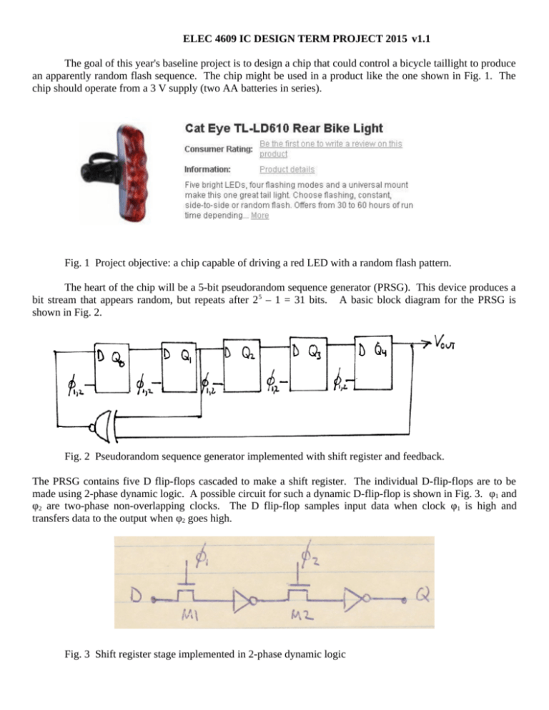
ELEC 4609 IC DESIGN TERM PROJECT 2015 v1.1 The goal of this year's baseline project is to design a chip that could control a bicycle taillight to produce an apparently random flash sequence. The chip might be used in a product like the one shown in Fig. 1. The chip should operate from a 3 V supply (two AA batteries in series). Fig. 1 Project objective: a chip capable of driving a red LED with a random flash pattern. The heart of the chip will be a 5-bit pseudorandom sequence generator (PRSG). This device produces a bit stream that appears random, but repeats after 2 5 – 1 = 31 bits. A basic block diagram for the PRSG is shown in Fig. 2. Fig. 2 Pseudorandom sequence generator implemented with shift register and feedback. The PRSG contains five D flip-flops cascaded to make a shift register. The individual D-flip-flops are to be made using 2-phase dynamic logic. A possible circuit for such a dynamic D-flip-flop is shown in Fig. 3. φ1 and φ2 are two-phase non-overlapping clocks. The D flip-flop samples input data when clock φ1 is high and transfers data to the output when φ2 goes high. Fig. 3 Shift register stage implemented in 2-phase dynamic logic Flip flops can also be made using static logic gates (see for example see http://en.wikipedia.org/wiki/Flip-flop_%28electronics%29#D_flip-flop or your ELEC2607 notes), but the dynamic approach provides a much more compact design. The D flip-flop of Fig. 3 stores information on the gate-channel capacitance of the transistors in the inverter stages. The length of time this charge is stored determines how long the flip-flop can hold data. For an SOI implementation the charge storage time is determined by off-state leakage through the transmission gates connecting the output of one inverter to the input of the next stage. Usually one would use full CMOS transmission gates to connect the inverters. The 4609 CMOS technology produces pMOS transistors that are likely to have high off-state leakage, so here we will use only nMOS transmission gates. Even with nMOS-only transmission gates, off-state leakage through M1 and M2 might be a problem due to the “floating body” effect in SOI. If M1 and M2 do not shut off completely when V GS = 0 the charge stored on the inverter input will be corrupted. This is a particular problem if the shift register is clocked slowly, as one would expect for a bicycle light. There are several ways to avoid or at least minimize this problem. The most compact solution uses a long T-gate structure (like that shown in Fig 4 below) for the transmission gate transistors M1 and M2. Fig. 4 T-gate nMOS layout (this will be discussed in class). The body (“B”) contact on the T-gate should be connected to VSS. A conceptually simpler solution (but one requiring more area) uses feedback to hold the flip-flop state, as shown in Fig. 5. It is very important that the feedback transistors M5, M6, M7… be long and narrow so that data does not flow in the reverse direction through the register. Fig. 5 Dynamic shift register with feedback. An even more robust solution to the leakage problem (requiring even more area) uses inverters in the feedback loop, as shown in Fig. 6. Fig. 6 Yet another dynamic shift register with feedback. I'd like to see some groups should use the T-gate solution, and others one of the “feedback” solutions. The PRSG requires an XNOR logic block. Designing a circuit schematic for this block is part of the project. Baker's textbook (and other sources) present some possible schematics. The PRSG of Fig. 2 can enter a “locked” state if every register holds a logic 1. To avoid entering this state, the PRSG needs a reset. The simplest reset would use a NOR gate in place of the second inverter in the final flip-flop stage in the shift register as suggested in Fig. 7. One input of the NOR gate would connect to an external reset line. When reset is asserted high, the output of the NOR gate could be forced low, producing a zero in the sequence. Fig. 7 Simple reset circuit (final stage in register). The 2-phase non-overlapping clocks φ1 and φ2 are required to drive the shift register. These clocks can be generated on chip using the circuit of Fig. 8. The cascaded inverters at the output of the NAND gates provide delay to ensure that φ1 and φ2 do not overlap. Fig. 8 2-phase generator A master clock generator is also required. Once again there are many possible astable circuits that can be used for clock generation. The basic clock generator circuit we will use is shown in Fig. 9. Fig. 9 Master clock generator- basic concept with external R and C setting frequency. To minimize the number of probe pads required, it is desirable to replace the external resistor with a non-linear resistive element synthesized from MOSFETs. This can be done as shown in Fig. 10, at the expense of a clock duty cycle significantly different from 50%. There may be better solutions for the clock generator- improved designs are welcome. The clock needs to be sufficiently slow that the LED flash rate is approximately 10 Hz. You are welcome to adjust the clock frequency slightly to arrive at the flash rate you think will be most visible. Fig. 10 Master clock generator, external R replaced by long, narrow MOSFET. The complete chip should include an output buffer able to drive a GaP red LED. A typical red LED has a turn-on voltage of about 2 V and draws 10 mA. The output buffer might consist of a single wide nMOS transistor in “open drain” configuration, as shown in Fig. 11. Fig. 11 Open drain output buffer If the clock generator fails, or if we wish to test at higher clock frequencies than can be provided by the oscillator of Fig. 10 an external clock can be injected at bond pad C2. Similarly, two "minipads" pads should be provided to inject 2-phase non-overlapping clocks to the shift register, if necessary. Minipads should be added anywhere else you think it might be desirable to override or test a signal. "Minipads" can be about 10 λ by 10 λ in size, and of course must be in metal. The complete project must fit in the floor plan shown in Fig. 12. The height of the project block is fixed at 240 λ, and must not be changed. The vertical position of the bond pad centers must also not be changed. The width of the project can be at most 240 λ. There will be rewards for minimizing width. Fig. 12 Probe pad placement and available area for layout Alternative Projects Alternative projects are possible. Some possibilities include: 1. Basic op-amp (only if you have taken ELEC3509, are currently taking ELEC4707 and have a strong interest in analog circuits). Using T-gate nMOS devices in the op-amp is highly recommended. 2. 4-bit binary counter with reset. 3. Test structures for SPICE Level 3 model parameter extraction. This project will include complete extraction of model parameters and comparison to experimental device characteristics. Contact your instructor if you wish to try one of these alternative projects. Project Management It is very important to make an early start on the project. A good approach is to complete the circuit schematics for each circuit block, and then confirm the operation of each block with extraction and SPICE simulation. Blocks would typically include a D flip-flop stage, XNOR, 2 phase clock generator, and master clock generator. A floorplan for the chip can then be drawn, showing the approximate placement of each block and the placement of the wiring to interconnect the blocks. Finally each block can be converted to layout using LEdit. MicroArt Contest Once again there will be a small prize for the best microart included with a project. The metal layer provides a shiny silver color, while poly and device well give more subtle green shades. Here is the winner from 2012:


