Workshop Program
Advance Program
5th IEEE International Workshop on Design for Manufacturability & Yield June, 6, 2011
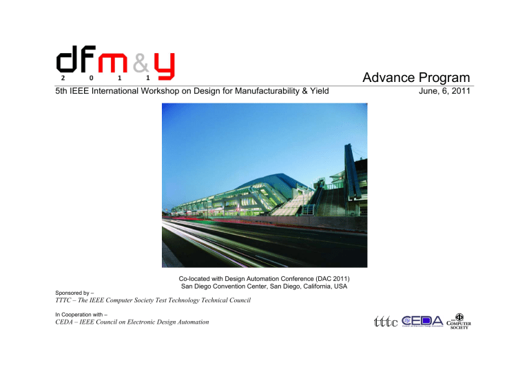
Co-located with Design Automation Conference (DAC 2011)
San Diego Convention Center, San Diego, California, USA
Sponsored by –
TTTC – The IEEE Computer Society Test Technology Technical Council
In Cooperation with –
CEDA – IEEE Council on Electronic Design Automation
MONDAY, JUNE 6, 2011
REGISTRATION , BREAKFAST: 8:30am - 8:50am
WELCOME REMARKS: 8:50am - 9:00am
Session 1: DESIGN-PATTERNING INTERACTIONS
9:00am - 10:30pm
Session Chair: Dr. Swamy Muddu, GlobalFoundries
1.1 <Invited Talk> Patterning Troubles for Standard
Cells
D. Pietromonaco, ARM
1.2 Parametric Hierarchy Recovery in Layout
Extracted Netlists
John Lee, Puneet Gupta and Fedor Pikus
1.3 Design Methodology to Compensate Transistor
Channel Length Litho-Induced Variations
Sergio Gomez, Francesc Moll, Lancelot
García-Leyva and Antonio Rubio
1.4 A Partitioning-Based Litho-Friendly SADP
Decomposition Method
Minoo Mirsaeedi, Andres Torres and Mohab Anis
COFFEE BREAK
10:30am – 10:50am
Session 2: CHARACTERIZATION OF VARIATION
10:50am – 12:00am
Session Chair: Dr. Mohamed Abu-Rahma, Qualcomm
2.1 <invited> System-Level Variability Measurement and Implications
Mani Srivastava, UCLA
2.2 Electrical Monitoring of Gate and Active Area
Mask Misalignment Error
Aditya Bansal, Amith Singhee, Emrah Acar and
Greg Costrini
2.3 A Stress-Parallelized Device Array for Efficient
Bias-Temperature Stability Measurement
Takashi Sato, Tadamichi Koazaki, Takumi Uezono,
Hiroshi Tsutsui and Hiroyuki Ochi
LUNCH AND INVITED TALK:
Transition from Planar MOSFETs to FinFETs and its
Impact on Design and Variability
12:00pm – 1:00pm
Speaker: V. Moroz, Synopsys
Session 3: STATISTICAL TREATMENT OF
VARIATION
1:00pm - 2:10pm
Session Chair: Prof. Costas Spanos, UC Berkley
3.1 <invited> Virtual Probe: A Statistical Framework for Low-Cost Variability Characterization of
Nanoscale Integrated Circuits
Xin Li, CMU
3.2 Techniques to Minimize VCCMIN Induced Yield
Loss in SRAM Arrays
Guru Shamanna, Raja Gaurav and Kshatri Bhunesh
3.3 Investigating the Effect of Adaptive Body
Biasing and Adaptive Voltage Scaling on
Parametric Yield in the Presence of Process and
Statistical Variability
Plamen Asenov, Dave Reid, Campbell Millar, Scott
Roy and Asen Asenov
BREAK AND POSTER SESSION
2:10pm – 3:00pm
P.1 Theory of Logical Partitioning for Yield/Area
Maximization using Redundancy
M. Mirza-Aghatabar, M. Breuer and S. Gupta
P.2 Power-awareness In DC EM Optimization
C.-M. Fu, C.-Y. Yu, P.-H. Yeh, Y.-T. Hou, W.-H.
Chen and T. Quan
P.3 An Integrated Schematic-Based Layout
Verification Flow Environment
S. Srinivasan, F. Pikus, P. Gibson and L. Ling
P.4 Design Margin Tightening Utilizing Local
Cancellation Effects with Stage-based OCV
W.-H. Chen, L.-Y. Du, Y.-T. Hou and T. Quan
P.5 Linear Propagation Methodology in Compact
Variability Modeling
Y. Qiao and C. J. Spanos
Session 4: TEST AND SYNTHESIS FOR YIELD
3:00pm - 4:20pm
Session Chair: Michael Orshansky, Univ. of Texas
4.1 <invited> DFM for Rapid Yield Ramp
Will Conley, Freescale
Variation Delay Defects
Vladimir Zolotov, IBM
4.3 Designing Approximate Circuits for
Error-Tolerant Applications to Improve
Performance Yield
Doochul Shin and Sandeep Gupta
PANEL DISCUSSION
What DFMY problem will you pay to get solved /
Where is the next DFMY startup?
4:20pm - 5:30pm
Organizer: Andrew Kahng
WORKSHOP SCOPE
Designing a SoC for manufacturability and yield must aim at improving the manufacturing process, and consequently its yield, by enhancing communications across the design–manufacturing interface. A wide range of
Design-for-Manufacturability (DFM) and Design-for-Yield
(DFY) methodologies and tools are proposed today. Some of these are leveraged during the back-end design stages, while others have post-design utilization, from lithography up to wafer sort, packaging, final test and failure analysis.
DFM can dramatically impact the business performance of chip manufacturers. It can also significantly affect age-old chip design flows. Using a DFM solution is an investment, and thus choosing the most cost-effective one(s) requires tradeoff analysis. This workshop analyzes key trends and challenges, and gives the opportunity to discuss a range of DFM and DFY solutions for today's SoC designs.
26,
2009
REGISTRATION
All workshop participants require registration. Please register at the following site. https://reg.mpassociates.com/reglive/PromoCode.aspx?c
onfid=122
WORKSHOP COMMITTEE
General Chair: R. Aitken, ARM
Program Chair: P. Gupta, UCLA
Publicity: J. Lu, UCSD
STEERING COMMITTEE
A. B. Kahng, UCSD
A. Singh, Auburn Univ.
Y. Zorian, Virage Logic
PROGRAM COMMITTEE
M. Abu-Rahma, Qualcomm
S. Datla, Texas Instruments
A. Gattiker, IBM
P. Gupta, UCLA
S. Gupta, USC
A. B. Kahng, UCSD
V. Moroz, Synopsys
N. S. Nagaraj, Texas Instruments
M. Orshansky, Univ. of Texas
D. Z. Pan, Univ. of Texas
C.-H. Park, Samsung
J. M. Portal, Univ. of Marseille
T. Quan, TSMC
M. S. Reorda, Politecnico di Torino
P. Sharma, Freescale
T. Shibuya, Fujitsu
A. Singhee, IBM
R. Topaloglu, GlobalFoundries
A. Torres, Mentor Graphics
