enter title here (14 pt type size, uppercased, bold and centered over
advertisement
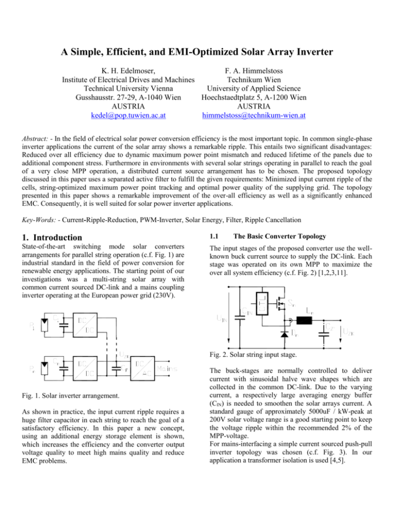
A Simple, Efficient, and EMI-Optimized Solar Array Inverter K. H. Edelmoser, F. A. Himmelstoss Institute of Electrical Drives and Machines Technikum Wien Technical University Vienna University of Applied Science Gusshausstr. 27-29, A-1040 Wien Hoechstaedtplatz 5, A-1200 Wien AUSTRIA AUSTRIA kedel@pop.tuwien.ac.at himmelstoss@technikum-wien.at Abstract: - In the field of electrical solar power conversion efficiency is the most important topic. In common single-phase inverter applications the current of the solar array shows a remarkable ripple. This entails two significant disadvantages: Reduced over all efficiency due to dynamic maximum power point mismatch and reduced lifetime of the panels due to additional component stress. Furthermore in environments with several solar strings operating in parallel to reach the goal of a very close MPP operation, a distributed current source arrangement has to be chosen. The proposed topology discussed in this paper uses a separated active filter to fulfill the given requirements: Minimized input current ripple of the cells, string-optimized maximum power point tracking and optimal power quality of the supplying grid. The topology presented in this paper shows a remarkable improvement of the over-all efficiency as well as a significantly enhanced EMC. Consequently, it is well suited for solar power inverter applications. Key-Words: - Current-Ripple-Reduction, PWM-Inverter, Solar Energy, Filter, Ripple Cancellation 1. Introduction 1.1 The Basic Converter Topology State-of-the-art switching mode solar converters arrangements for parallel string operation (c.f. Fig. 1) are industrial standard in the field of power conversion for renewable energy applications. The starting point of our investigations was a multi-string solar array with common current sourced DC-link and a mains coupling inverter operating at the European power grid (230V). The input stages of the proposed converter use the wellknown buck current source to supply the DC-link. Each stage was operated on its own MPP to maximize the over all system efficiency (c.f. Fig. 2) [1,2,3,11]. Fig. 2. Solar string input stage. Fig. 1. Solar inverter arrangement. As shown in practice, the input current ripple requires a huge filter capacitor in each string to reach the goal of a satisfactory efficiency. In this paper a new concept, using an additional energy storage element is shown, which increases the efficiency and the converter output voltage quality to meet high mains quality and reduce EMC problems. The buck-stages are normally controlled to deliver current with sinusoidal halve wave shapes which are collected in the common DC-link. Due to the varying current, a respectively large averaging energy buffer (CIN) is needed to smoothen the solar arrays current. A standard gauge of approximately 5000uF / kW-peak at 200V solar voltage range is a good starting point to keep the voltage ripple within the recommended 2% of the MPP-voltage. For mains-interfacing a simple current sourced push-pull inverter topology was chosen (c.f. Fig. 3). In our application a transformer isolation is used [4,5]. U IN U DC i1 RL1 RL 2 RO R R R R R R L1 L 2 L t L1 L 2 L t LS 1 LS 2 LO 1 e iAB e LS 1 LS 2 LO . (6) 1.2 Fig. 3. Inverter stage. To clarify the current ripple problematic the structure given in Fig. 3 was modeled in SPICE and simulated. For this simplified model a 1:32-transformer was used. The simulation results of the topology (input voltage: 12V, load resistance: 1kΩ, duty cycle: 50%) are shown in Fig. 5. 400 200 0 -200 -400 0 0.2 0.4 0.6 0.8 10 1 x 10 -4 0 I(S1) [A] -10 15 10 5 0 -5 I(S2) [A] U(TR) [V] U(OUT) [V] As can be seen from Fig. 3, the structure is very similar to the standard boost-converter. Simulation of the push-pull inverter 15 10 5 0 -5 0 0.2 0.4 0.6 0.8 1 x 10 0 0.2 0.4 0.6 0.8 1 x 10 0 0.2 0.4 0.6 -4 -4 0.8 1 x 10 -4 Fig. 5. Simulation: from top to bottom: output voltage, voltage across one primary, current through the switches S1 & S2. For each operation state the system equations can be given: di1 LS1 LS1 LO , (2) dt R R R L1 L 2 L t LS 1 LS 2 LO iAB e R R R L1 L 2 L t LS 1 LS 2 LO (3) UTR ( U L1 ) U IN , U IN U DC i1 RL1 RL1 RO (4) di1 LS1 LS1 LO dt I(S1) , 0 0.2 0.4 0.6 0.8 1 x 10 0 0.2 0.4 0.6 0.8 20 1 x 10 (5) -4 10 0 20 0 0.2 0.4 0.6 0.8 1 x 10 -4 0 -20 0 0.2 0.4 0.6 0.8 1 x 10 , -4 0 -2 VG(S1,S2) 1 e 0 -10 V(S1) (1) U IN U DC i1 RL1 RL1 RO U IN U DC RL1 RL 2 RO 10 2 UTR ( U L1 ) U IN , i1 V(OUT) Fig. 4. Operational principle of the converter. -4 Fig. 6. Simulation from top to bottom: output voltage, transformer current (here magnetizing current), voltage across one switch, control signal of the switches. V(OUT) For the sake of clarity and to show the influence of the magnetizing current, a transformer ratio of 1:1 is chosen in Figs. 5 & 6. Figure 7 shows the simulation results at no load condition of the converter, while Fig. 8 depicts a 12A load condition (1Ω load). The magnetizing current can be seen clearly in both cases. Some comparing measurements of a 1.2kW (10 cells operating in series connection) test array show the influence of the input capacitor of the solar converter. Table 1 clarifies the problematic and shows the efficiency derating. Lifetime reduction will effect the plant MTBF and are not be taken into considerations here. 10 0 CIN -10 I(S1) 0 V(S1) 0.2 0.4 0.6 0.8 15 10 5 0 1 x 10 0 0.2 0.4 0.6 0.8 20 -4 1 x 10 -4 10 0 VG(S1,S2) 2. The input current ripple problem 20 0 0.2 0.4 0.6 0.8 1 x 10 -4 0 -20 0 0.2 0.4 0.6 0.8 PAVG Eff. 100μF 885W 73.7% 200μF 1085W 90.4% 500μF 1180W 98.3% 1000μF 1195W 99.5% 5000μF 1198W 99.8% *) 10000μF 1200W 100,00% *) Table 1 Efficiency derating due to MPP mismatch (* ripple below 2% as recommended by manufactory) 1 x 10 -4 VDC (OUT) Fig. 7. Simulation from top to bottom: output voltage, transformer current (magnetizing plus transformed load current), voltage across one switch, control signal of the switches. (discontinuous mode). 5 I(S1) 0 3 2 1 0 -1 V(S1) 30 9.2 9.4 9.6 9.8 10 x 10 9 9.2 9.4 9.6 9.8 -4 10 x 10 20 -4 10 0 VG(S1,S2) 9 20 9 9.2 9.4 9.6 9.8 10 x 10 -4 0 -20 9 9.2 9.4 9.6 9.8 10 x 10 -4 Fig. 8. Simulation from top to bottom: output voltage, switch current (magnetizing plus transformed load current), voltage across one switch, control signal of the switches. (inductive load). Fig. 9. Simulated system behavior of the input stage: (from top to bot.) Input current, array voltage (=UIN), solar energy, storage capacitor’s (CIN) energy. Figure 9 shows simulation results of the input stage without any active filtering. The solar cells are buffered with 5000uF to fulfill the manufacturer’s requirement of 2% voltage ripple. To overcome the problem of energy storage in each input cell, an improved topology with shared storage elements was derived. An additional energy storage cell operating at the same DC-link was used to smoothen the input current ripple (c.f. Fig. 10) be used without any disadvantage to the circuit behaviour. (ref.: ΔWC=C.U.ΔU). To reach the given topics a simple filter structure based on a storage capacitor and a bidirectional DC/DC converter was chosen (c.f. Fig. 11). The control principle used of this filter is based on a simple current mode regulator fed from a common load regulation unit with the goal of mains ripple elimination in the solar string. 3. Modeling of the compensator Fig. 10. Improved inverter topology with active filter The parameters of the model are the link capacitor CZK, its series resistor RCZ, the capacitor of the active filter CB, its series resistor RB, the inductor LB, its series resistor RLB, the on-resistors of the upper RSBU and the lower RSBL active switch. The state variables are the inductor current iLB , the capacitor voltage of the buffer capacitor uCB, and the capacitor voltage of the filter capacitor uCF. The input variables are the output currents of the DC-to-DC converters i1 .. iN , and the input current of the inverters DC-link iZK. In continuous inductor current mode there are two states. In state one the upper active switch SBU is turned on and the second (lower) active switch SBL is turned off. Figure 12 shows this switching state one. The state space equations are now diLB 1 dt LB iLB RCB RCZ RLB RSBU uCB uCK RCZ i1 .....iN iZK (7) Fig. 11. Active filter circuitry The simple principle of current summation was used in combination of an energy storage at higher voltage levels (in our case 400V) (ref.: WC=C*U2/2). Also a much higher voltage ripple across the filter capacitor can RCB RCZ RLB RSBU LB iLB d 1 uCB dt CB uCZ 1 CZK 1 LB 0 0 1 RCZ LB iLB LB 0 uCB 0 u 1 CZ CZK 0 duCB iLB dt CB (8) d u iB i . . . . . i i C Z 1 N Z K L d t C B (9) leading to the state space description given in equation 10. RCZ LB 0 1 CZK RCZ i1 LB . . . 0 . . 1 iN . . CZK iZK . . (10) In state two the upper active switch SBU is turned off and the lower SBL switch is turned on. Figure 13 shows this switching state two. Combining the two systems by the state-space averaging method leads to a model, which describes the converter (active filter) in the mean. On condition that the system time constants are large compared to the switching period, we can combine these two sets of equations. Weighed by the duty ratio, the combination of the two sets yields to equation 15. By this matrix equation the dynamic behaviour of the converter is described correctly in the average, thus quickly giving us a general view of the dynamic behaviour of the converter. The superimposed ripple (which appears very pronounced in the coil) is of no importance for qualifying the dynamic behaviour. This model is also appropriate as large-signal model, because no limitations with respect to the signal values have been made. Fig. 12. Switching state one: driving state The weighed matrix differential equation representing the dynamic behavior of the converter is a nonlinear one. To use the possibilities of the linear control theory, a linearization of the state matrix is necessary. With capital letters for the operating point values and small letters for the disturbance around the operating point Fig. 13. Switching state two: freewheeling phase of the power stage The describing equations are diLB 1 iLB RCZ RLB RSBL uCK dt LB RCZ i1 .....iN iZK du CB 0 dt duCZ iLB i1 .....iN iZK dt CB iLB I LB 0 i LB (11) (16) uCB U CB 0 u CB (17) (12) d D0 d (13) one can calculate the linearized small signal model of the converter according to equation 19. (18) leading to the systems state space description given in equation 14. RCZ RLB RSBL LB iLB d uCB 0 dt 1 uCZ CZK 0 0 0 1 LB iLB 0 uCB u 0 CZ ( RCB RSBU ) d RCZ RLB RSBL (1 d ) LB iLB d d u CB dt CB uCZ 1 CZK RCZ L B 0 1 CZK d LB 0 0 RCZ LB 0 1 CZK RCZ i1 LB . . . 0 . . 1 iN . . CZK iZK . . 1 RCZ LB L i LB B 0 uCB 0 u 1 CZ CZK 0 RCZ LB 0 1 CZK RCZ i1 LB . . . 0 . . 1 iN . . CZK iZK (14) . . (15) ( RCB RSBU ) D0 RCZ RLB RSBL (1 D0 ) LB i LB D0 d u CB dt CB u CZ 1 CZK RCZ LB 0 1 CZK RCZ LB 0 1 CZK R . . CZ LB . . 0 . . 1 CZK D0 LB 0 0 1 LB i LB 0 u CB u CZ 0 (19) ( RCB RSBU RSBL ) I LB 0 U CB 0 i1 . LB . I LB 0 i . CB N iZK 0 d parallel to the panels are necessary to bridge a gap of the maximum length of the converter switching period, the inverse of the converter switching frequency fs 4. Capacitor estimation Using capacitors in parallel to the solar panel alone we have an input current of a single converter according iIN I sin t . (20) The mean value of the input current should be the optimum power point current of the panel and can be calculated to I 2 . C uIN fs (26) Taking for example a switching frequency fs = 50kHz the necessary parallel capacitor is I C12 ,7 F. uIN (27) T /2 _ 2 2 I Isin tdt I. T0 (21) The necessary capacitor to avoid higher voltage variation then u IN has to be calculated with t 1 2 I 2 , C sin t dt u IN 0 (22) with 1 2 t1 arcsin 2 f (23) and is therefore 2 I 1 2 2 2 . C arcsin 1 1 u f IN (24) In the 50 Hz mains one can write the dimensioning equation I . C1 ,34 mF uIN (25) With n panels n such capacitors are necessary. Using the maximum power point current as constant input current of the converters, only small capacitors in Fig. 14. Relationship of C /(C B n I ) to the factors m (higher voltage level) and a (increased voltage ripple ). Storing the energy at a factor m higher voltage level and a a-times higher voltage ripple, one needs a storage capacitor of n I . CB C m a (28) In Fig. 14 it can be seen that a increased voltage ripple and higher DC-link voltage will lead to significantly reduced capacitor requirements. To clarify this behavior an example arrangement of eight solar strings, each operating at UMPP=44V, delivering PS=240W and supported with an active Filter stage with CB=1000μF, is simulated to show the input voltage ripple ratio UINR/UBR for varying filter voltages UB and input capacitors C. The relationship can be estimated to UB U IN U INR CB . U BR C n I 5. Simulation of the compensator To clarify the filter operation a sample arrangement of solar strings, each consisting of ten solar modules (Kyocera KC-120-2) are modeled. The strings are controlled separately for MPP operation and fed into a 120V DC-link. For the mains interface a simple transformer coupled inverter (c.f. Fig. 3) is used. In our case a system as depicted in Fig. 10 with a current mode controlled active filter stage shown in Fig. 11 was treated in detail. The filter was operated at UB=400V, a switching frequency of 25kHz was chosen for minimum EMC-problematic and switching losses. The figures 16 and 17 depict the mathematical simulation results of the operating filter for two intervention levels. (29) Fig. 15 Voltage ripple relationship UINR/UBR depending on input capacitor C and filter voltage level UB. As one can see in Fig. 15 an active filter operating at more than six times the input voltage (approximately 250V in our case) will lead to a satisfactory input current ripple suppression. Higher voltage levels can help to reduce the system requirements compared to a conventional solution or improve the system behavior leading to a significantly reduced component stress in the cells. By using a filter voltage level of 400V a ripple reduction of more than 70% (compared to 250V) can be achieved when the same components are used. Fig. 16. Filter behavior, 100% compensation (from top to bot.): Input voltage, array current, buffer capacitor’s current, compensator & load current. Figure 16 shows full compensation. Here no lowfrequency ripple can be found in the input capacitor’s (we assumed 200uF) current – only switching ripple occurs. The over-all efficiency (as well as the MPPefficiency) of the system reaches 99% in this case. Contrary to this case in Fig. 17 the results of a 50% compensated system are depicted. Due to the input current ripple, the resulting MPP mismatch leads to a reduction of about 6% of the over all efficiency. To show the further benefits of using an active cancellation filter the DC-link current spectrum was taken into considerations. As one can see in Fig. 18 the optimal usage of the filter stage can help to reduce the EMC problematic of the solar arrangement when also harmonics cancellation algorithms are used. Hard Switching Leg 2 10 I(DLC) [A] 1 10 0 10 -1 10 3 10 4 5 10 10 6 10 Advanced Structure 2 10 I(DCL) [A] 1 10 0 10 Fig. 17. Filter behavior, 50% compensation (from top to bot.): Input voltage, array current, buffer capacitor’s current, compensator & load current. -1 10 3 10 4 5 10 10 6 10 f[Hz] Two further aspects gave us the potential of additional improvements: The input stages can be operated in phase shift mode at the same carrier frequency leading to a significantly improved ripple current in the DC-link. This can help to minimize ripple cancellation capacitors and additional switching frequency filter elements. It has to be noted that in this case a dedicated controller is required to guarantee optimal phase delay depending on available stages. Another interesting aspect is the capability of active harmonics cancellation by using a dedicated filter algorithm. In the previous discussed sections we used the filter only to eliminate current ripple of the solar cells (our filter was only used as a special storage cell to eliminate the mains current pulsation). The filter stage is operated at 25kHz, so there was enough potential also to implement a harmonics filter for the DC-to-AC inverter. Fig. 18. DC-link current spectrum (EMC) comparison of a conventional topology (upper figure) and the advanced structure using an active filter (lower figure). Figure 19 depicts the influence of phase number and duty cycle on the output current ripple of a multiphase arrangement. For generalization in the graph, the output current ripple ICR,PP is normalized against the inductor current ripple of one inverter stage at zero duty cycle V ICR K O . ,PP L bf (29) In figure 20 one can see the RMS input current ripple IICR,RMS depending on duty cycle for different phase arrangements. In this graph, the RMS input current ripple of the step down cell (c.f. Fig. 2) is normalized against the DC-link current IDCL. The duty-cycle depends on the relationship of input / output voltage, in our example varying in the range from 10 to 90 percent. Consequently, there exists an optimum phase number to achieve the minimum RMS input current ripple for a fixed input and output application. For a wide duty cycle range application, higher phase number helps to reduce the maximum input current ripple. But the reduction in the input current ripple by increasing phase number may not be significant at higher phase numbers in certain duty cycle ranges. The optimum phase number needs to be evaluated over the complete operating duty cycle range. It should once more be noted, that a ripple reduction directly affects the component stress in the solar cells. 6. Conclusion Fig. 19. Normalized output current ripple factor K vs converter duty cycle DC, shown for 1 (blue), 2 (cyan), 3 (magenta), 4(green), and 8 (black) phase step down configurations. Fig. 20. Normalized RMS input current ripple ICR,RMS vs duty cycle DC, shown for 1 (blue), 2 (cyan), 3 (magenta), 4(green), and 8 (black) phase inverter configurations. The proposed solution improves efficiency as well as component reliability in solar-, fuel cell- and battery fed inverter applications by an active reduction of the source current ripple. As a result the source is only loaded with a perfect DC-current, which helps to hit the maximum power point without any dynamic distortions. Furthermore, the input capacitor can be decreased, because a common energy storage element is used operating at higher voltages with higher efficiency. As shown in Fig. 10 the approach can be used to optimize the as well as the system behaviour and the over-all efficiency. It should be noted, that for optimum plant efficiency a load sharing control system should be established. The simple principle of the parallel operation of controlled current sources forms a robust and fault-tolerant system. The proposed topology can be used as an alternative to multi-stage converters with a constant DC-link voltage and an active switching DC-toAC inverter. The power stage of the used filter consists of a simple half bridge arrangement feeding the ripple current. The converter is operated at several 10kHz leading to a tolerable low output current ripple. Cheap TO-247 or even TO-220 or cheap surface mount packages can be used leading to a compact and efficient system design [6,7,8,9,10]. The effective usage of multi-phase input cells coupled with an active filter show us the capability to reach the goal of high efficiency, reduced current harmonics and improved EMC. Furthermore it should be noted that the parallel structures are forming a redundant system which can be used to increase the systems reliability by building a fault tolerant arrangement. All these advantages can simply be realized in software and do not affect the hardware. The simple control principle of the power stages can easily be implemented using state-of-the-art microcontrollers without additional logic support for the pulse pattern generator; a simple PWM stage fulfills all the requirements. Also the maximum power point tracking for the solar generator can be easily implemented by monitoring the system signals (i1 .. iN , and iZK.). The topology presented in this paper is a simple and effective solution for small to medium power grid coupled applications. The concept is well suited for wind-, solar- and renewable energy as well as for aerospace applications. References: [1] Wai, R; Lin, C: “Active Low-Frequency Ripple Control for Clean-Energy Power Conditioning Mechanism”, Proceedings of the IEEE Transactions on Industrial Electronics 1-2010, Vol.: PP , Issue: 99, pp.: 1-10 [2] Veerachary, M.; Senjyu, T.; Uezato, K.: “Maximum power point tracking control of IDB converter supplied PV system”, Proceedings of the IEE Electric Power Applications 2001, Vol.: 148 , Issue: 6, pp.: 494 - 502 [3] Duran, E.; Galan, J.; Sidrach-de-Cardona, M.; Segura, F.: “An application of interleaved DC-DC converters to obtain I-V characteristic curves of photovoltaic modules”, Proceedings of the 34th IEEE Annual Conference of Industrial Electronics, IECON 2008, pp.: 2284 - 2289 [4] Hung, J.-C.; Wu, T.-F.; Tsai, J.-Z.; Tsai, C.-T.; Chen, Y.-M.: “An active-clamp push-pull converter for battery sourcing applications”, Proceedings of the Twentieth Annual IEEE Applied Power Electronics Conference and Exposition, APEC 2005. Volume 2, March 6-10, 2005, pp.1186-1192. [5] Edelmoser, K. H;. Ertl, H.: "DC-to-DC Converter for Low Voltage Solar Applications", Proceedings of the 11th WSEAS International Conference on Circuits, Systems, Communications and Computers CSCC '07, Circuit Theory and Applications, July 23.-28. 2007, Ag. Nicolaos, Greece, ISBN: 978-960-8457-89-8, pp.: 104108. [6] K. H. Edelmoser, F. C. Zach: "DC-to-DC Converter With Extended Voltage Transfer Ratio, Optimized for Bi-Directional Operation", WSEAS Transactions on Power Systems, Issue 6, Volume 1, June 2006, ISSN: 1790-5060, pp.: 1057-1061. [7] K. H. Edelmoser: "Common Mode Problematic of Solar Inverter Systems", Proceedings of the 10th WSEAS International Conference on Circuits, Systems, Communications and Computers CSCC '07, Circuit Theory and Applications, July 23.-28. 2007, Ag. Nicolaos, Greece, CD-ROM, ISBN: 978-960-8457-89-8, pp.: 131 – 135. [8] K. H. Edelmoser: "Three Level DC-to-AC Power Inverter for Power Grid Operation ", Proceedings of the 7th WSEAS International Conference on Circuits, Systems, Communications and Computers CSCC '05, July 11.-16. 2004, Athen, Greece, CD-ROM, ISBN: 9608457-29-7, 497-295.pdf. [9] K. H. Edelmoser, F. A. Himmelstoss: "Efficiency Optimized, EMI-Reduced Solar Inverter Power Stage ", Proceedings of the 11th WSEAS International Conference on Circuits, Systems, Communications and Computers CSCC '08, Heraklion, Greece, July 22-24, 2008. ISBN: 978-960-6766-82-4. 193. ISSN: 1790-5117 [10] K. H. Edelmoser, H. Ertl, F. C. Zach: "A Multi-Cell Switch-Mode Power-Supply Concept Featuring Inherent Input Voltage Balancing", Proceedings of the 10th WSEAS International Conference on Circuits, Systems, Communications and Computers CSCC '06, July 10.-15. 2006, Athen, Greece, CD-ROM, ISBN:960-8457-47-5, 534-373.pdf. [11] K. H. Edelmoser, F. A. Himmelstoss: “DC-to-DC Solar Converter with Controlled Active Clamping System”, Proceedings of the 12th International Power Electronics and Motion Control Conference (EPE-PEMC 2006), August 30 - September 1, 2006, Portoroz, Slovenia, pp.: 124-129.

