Word
advertisement
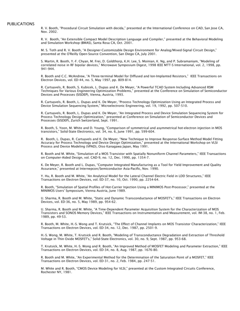
PUBLICATIONS R. V. Booth, “Procedural Circuit Simulation with decida,” presented at the International Conference on CAD, San Jose CA, Nov. 2002. R. V. Booth, “An Extensible Compact Model Description Language and Compiler,” presented at the Behavioral Modeling and Simulation Workshop (BMAS), Santa Rosa CA, Oct. 2001. M. S. Toth and R. V. Booth, “A Designer-Customizable Design Environment for Analog/Mixed-Signal Circuit Design,” presented at the O'Reilly Open-Source Convention, San Diego CA, July 2001. S. Martin, R. Booth, Y.-F. Chyan, M. Frei, D. Goldthorp, K.H. Lee, S. Moinian, K. Ng, and P. Subramaniam, “Modeling of correlated noise in RF bipolar devices,” Microwave Symposium Digest, 1998 IEEE MTT-S International, vol. 2, 1998, pp. 941-944. R. Booth and C.C. McAndrew, “A Three-terminal Model for Diffused and Ion-Implanted Resistors,” IEEE Transactions on Electron Devices, vol. ED-44, no. 5, May 1997, pp. 809-814. R. Cartuyvels, R. Booth, S. Kubicek, L. Dupas and K. De Meyer, “A Powerful TCAD System Including Advanced RSM Techniques for Various Engineering Optimization Problems,” presented at the Conference on Simulation of Semiconductor Devices and Processes (SISDEP), Vienna, Austria, 1993. R. Cartuyvels, R. Booth, L. Dupas and K. De Meyer, “Process Technology Optimization Using an Integrated Process and Device Simulation Sequencing System,” Microelectronic Engineering, vol. 19, 1992, pp. 507-510. R. Cartuyvels, R. Booth, L. Dupas and K. De Meyer, “An Integrated Process and Device Simulation Sequencing System for Process Technology Design Optimization,” presented at Conference on Simulation of Semiconductor Devices and Processes (SISDEP), Zurich Switzerland, Sept. 1991. R. Booth, S. Yoon, M. White and D. Young, “Comparison of symmetrical and asymmetrical hot-electron injection in MOS transistors,” Solid-State Electronics, vol. 34, no. 6, June 1991, pp. 599-604. R. Booth, L. Dupas, R. Cartuyvels and K. De Meyer, “New Technique to Improve Response-Surface Method Model Fitting Accuracy for Process Technology and Device Design Optimization,” presented at the International Workshop on VLSI Process and Device Modeling (VPAD), Oiso Kanagawa Japan, May 1991. R. Booth and M. White, “Simulation of a MOS Transistor with Spatially Nonuniform Channel Parameters,” IEEE Transactions on Computer-Aided Design, vol. CAD-9, no. 12, Dec. 1990, pp. 1354-7. K. De Meyer, R. Booth and L. Dupas, “Computer Integrated Manufacturing as a Tool for Yield Improvement and Quality Assurance,” presented at Internepcon/Semiconductor Asia-Pacific, Nov. 1990. Y. Hu, R. Booth and M. White, “An Analytical Model for the Lateral Channel Electric Field in LDD Structures,” IEEE Transactions on Electron Devices, vol. ED-37, no. 10, Oct. 1990, pp. 2254-64. R. Booth, “Simulation of Spatial Profiles of Hot-Carrier Injection Using a MINIMOS Post-Processor,” presented at the MINIMOS Users' Symposium, Vienna Austria, June 1989. U. Sharma, R. Booth and M. White, “Static and Dynamic Transconductance of MOSFET's,” IEEE Transactions on Electron Devices, vol. ED-36, no. 5, May 1989, pp. 954-62. U. Sharma, R. Booth and M. White, “A Time-Dependent Parameter Acquisition System for the Characterization of MOS Transistors and SONOS Memory Devices,” IEEE Transactions on Instrumentation and Measurement, vol. IM-38, no. 1, Feb. 1989, pp. 49-53. R. Booth, M. White, H.-S. Wong and T. Krutsick, “The Effect of Channel Implants on MOS Transistor Characterization,” IEEE Transactions on Electron Devices, vol. ED-34, no. 12, Dec. 1987, pp. 2501-9. H.-S. Wong, M. White, T. Krutsick and R. Booth, “Modeling of Transconductance Degradation and Extraction of Threshold Voltage in Thin Oxide MOSFET's,” Solid-State Electronics, vol. 30, no. 9, Sept. 1987, pp. 953-68. T. Krutsick, M. White, H.-S. Wong and R. Booth, “An Improved Method of MOSFET Modeling and Parameter Extraction,” IEEE Transactions on Electron Devices, vol. ED-34, no. 8, Aug. 1987, pp. 1676-80. R. Booth and M. White, “An Experimental Method for the Determination of the Saturation Point of a MOSFET,” IEEE Transactions on Electron Devices, vol. ED-31, no. 2, Feb. 1984, pp. 247-51. M. White and R. Booth, “CMOS Device Modeling for VLSI,” presented at the Custom Integrated Circuits Conference, Rochester NY, 1981. TECHNICAL MEMORANDA 1. A 3-Terminal Model for Diffused and Ion-Implanted Resistors 2. N-Section R-C Models for Integrated Resistors 3. The AUSSIM MOSFET Model 4. The RSIM MOSFET Model 5. S-Parameter Measurements and Modeling for 0.25mm MOSFET’s 6. The AMC Compact Model Compiler 7. The Effect of Feed-back Delay on the Noise Response of the Phase-Locked Loop 8. Analog and Simple Behavioral Verilog Models for the Dual-Loop Phase-Locked Loop 9. Clock Signal Jitter Metrics 10. PLL stability at low ratios of phase-detector frequency to PLL bandwidth 11. Crystal-oscillator simulation using a Q-controllable behavioral crystal model PATENT SUBMISSIONS 1. A 50% duty-cycle preserving 1 to 8 divider cell which requires no reset 2. Voltage-controlled oscillator delay cell for phase-locked loop 3. Loop Filter for Use in a Phase-Locked Loop: United States Patent 7,026,879 April 11, 2006 4. Cross-Fill Pattern for Metal Fill Levels, Power-Supply Filtering, and Analog Circuit Shielding: United States Patent 7037,820 May 2, 2006 5. Software and methodology for schematics-based full-chip place-and-route layout 6. Signal Generator with Selectable Mode Control: United States Patent 7,042,258 May 9, 2006 7. Glitchless clock and levels MUX that is frequency independent and does not need inputs to be synchronous or have integer relationships 8. Unit-cell layout technique for current-mirror components 9. Switch-Sequencing Circuits: United States Patent 7,521,969 April 21, 2009 10. A global reference current distribution scheme with programmable bias controls and compensation for process, voltage and temperature variations. 11. Differential output buffer with switched internal load to maintain common-mode feedback steady-state during disable state 12. Programmable Divider with relative Phase Delay or Advance for PLLs with Multiple Outputs: United States Patent 7,586,344 September 8, 2009 13. Combined Variable Gain Amplifier and Analog Equalizer Circuit 14. Shared-Array Multiple-Output Digital to Analog Converter 15. Method of delaying data from clock in 1UI steps 16. Expandable shift-register for Decision-Feedback Equalizer 17. Phase-locked loop circuit with selectable feedback paths 18. Power control block with output glitch protection
