ECE_SEM_1_ENGG_GRAPHICS_CLASS_NOTES_1
advertisement
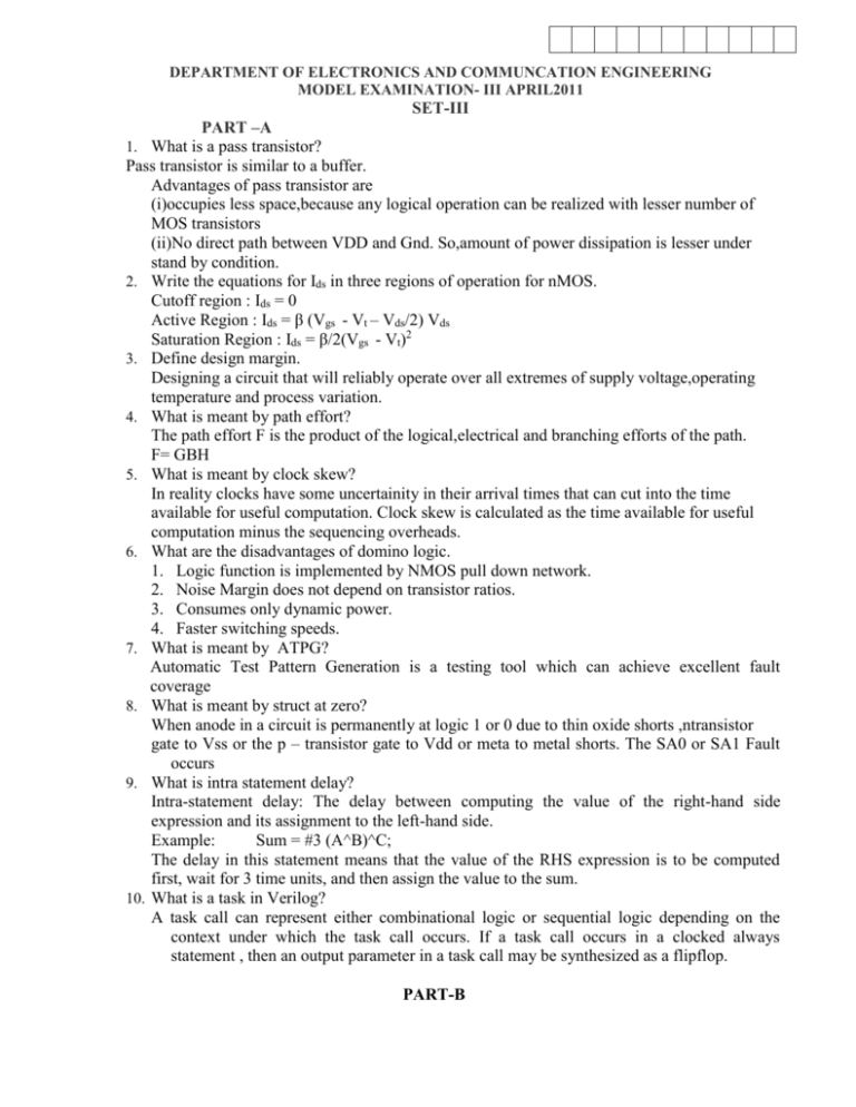
DEPARTMENT OF ELECTRONICS AND COMMUNCATION ENGINEERING MODEL EXAMINATION- III APRIL2011 SET-III PART –A 1. What is a pass transistor? Pass transistor is similar to a buffer. Advantages of pass transistor are (i)occupies less space,because any logical operation can be realized with lesser number of MOS transistors (ii)No direct path between VDD and Gnd. So,amount of power dissipation is lesser under stand by condition. 2. Write the equations for Ids in three regions of operation for nMOS. Cutoff region : Ids = 0 Active Region : Ids = β (Vgs - Vt – Vds/2) Vds Saturation Region : Ids = β/2(Vgs - Vt)2 3. Define design margin. Designing a circuit that will reliably operate over all extremes of supply voltage,operating temperature and process variation. 4. What is meant by path effort? The path effort F is the product of the logical,electrical and branching efforts of the path. F= GBH 5. What is meant by clock skew? In reality clocks have some uncertainity in their arrival times that can cut into the time available for useful computation. Clock skew is calculated as the time available for useful computation minus the sequencing overheads. 6. What are the disadvantages of domino logic. 1. Logic function is implemented by NMOS pull down network. 2. Noise Margin does not depend on transistor ratios. 3. Consumes only dynamic power. 4. Faster switching speeds. 7. What is meant by ATPG? Automatic Test Pattern Generation is a testing tool which can achieve excellent fault coverage 8. What is meant by struct at zero? When anode in a circuit is permanently at logic 1 or 0 due to thin oxide shorts ,ntransistor gate to Vss or the p – transistor gate to Vdd or meta to metal shorts. The SA0 or SA1 Fault occurs 9. What is intra statement delay? Intra-statement delay: The delay between computing the value of the right-hand side expression and its assignment to the left-hand side. Example: Sum = #3 (A^B)^C; The delay in this statement means that the value of the RHS expression is to be computed first, wait for 3 time units, and then assign the value to the sum. 10. What is a task in Verilog? A task call can represent either combinational logic or sequential logic depending on the context under which the task call occurs. If a task call occurs in a clocked always statement , then an output parameter in a task call may be synthesized as a flipflop. PART-B 11. a. (i) Explain with neat diagram CMOS inverter DC transfer characteristics. Refer notes (ii) Explain SOI disadvantages Refer notes (b) Explain in detail n-well process in CMOS technology. 1. Wafer formation 2. Photolithography 3. Well and channel formation 4. Silicon di oxide 5. Isolation 6. Gate oxide 7. gate and source/drain formation 8. Contacts and metallization 12. a. (i) Explain in detail CMOS process enhancement . Transistors: 1. Multiple threshold voltages & Oxide thickness 2. SOI process 3. Pass gate leakage mechanism 4. High K dielectrics 5. Low Leakage transistors 6. Higher Mobility 7. Plastic Transistors 8. High Voltage Transistors Interconnect Circuit Elements b. (i) Explain Reliability in detail. Electro migration : High current densities lead to an electron wind that causes metal atom to migrate over time. It causes wearout of metal interconnect through formation of voids Self Heating: It causes temp induced electro migration problem in bidirectional wires. Brief pulses of high peak current may melt the interconnect Significant for SOI process Hot Carriers As transistors switch,high energy (hot) carriers may be injected into the gate oxide and trapped. The damaged oxide changes I- V characteristics of the device decreases current in nMOS and increases current in pMOS Worst for inverters and NOR gates. Latch Up Overvoltage Failure Electrostatic Discharge Oxide Breakdown Punchthrough Time dependent dielectric failure Soft Errors CIRCUIT PITFALLS Threshold Drops Ratio Failures Leakage Charge Sharing Power Supply Noise Hot Spots Minority Carrier injection Back gate coupling Diffusion input noise immunity Process Sensitivity 13. a.. Explain synchronizers in detail: Theory refer notes . (or) b. Explain the following in detail with respect to sequencing static circuits. (i) Max-delay constraint (ii) Min-delay constraint (iii) Time borrowing 14. a. (i)Explain in detail manufacturing test principles. Refer notes b. (i) Explain BIST in detail. Refer notes (ii) Explain IDDQ testing . Refer notes 15. a.(i) Explain in detail procedural assignments.(Refer notes) (ii) Give the different types of gate delays present in Verilog. The signal propagation delay from any gate input to the gate output can be specified using a gate delay. Types of Gate Delay 1.Rise Delay 2.Fall Delay 3.Turn- Off delay b.(i) Explain in detail switch level modeling Refer notes (ii)Write a Verilog program for 3 bit priority encoder Refer notes
