Optical Interconnection Networks: The OSMOSIS Project
advertisement

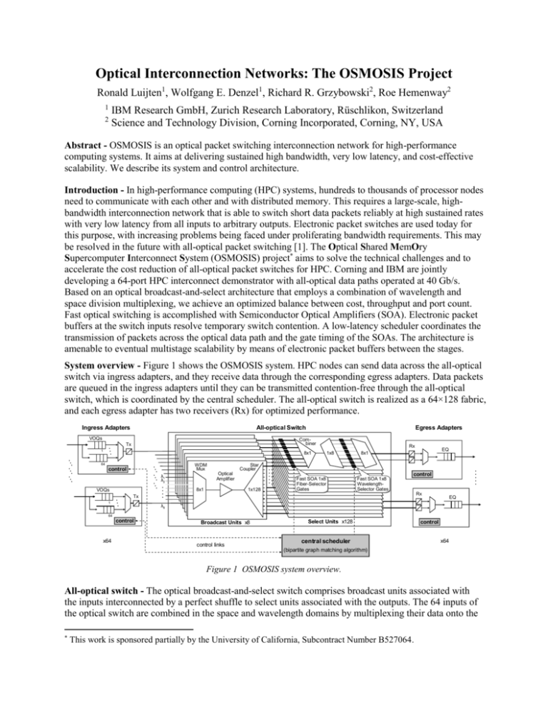
Optical Interconnection Networks: The OSMOSIS Project Ronald Luijten1, Wolfgang E. Denzel1, Richard R. Grzybowski2, Roe Hemenway2 1 2 IBM Research GmbH, Zurich Research Laboratory, Rüschlikon, Switzerland Science and Technology Division, Corning Incorporated, Corning, NY, USA Abstract - OSMOSIS is an optical packet switching interconnection network for high-performance computing systems. It aims at delivering sustained high bandwidth, very low latency, and cost-effective scalability. We describe its system and control architecture. Introduction - In high-performance computing (HPC) systems, hundreds to thousands of processor nodes need to communicate with each other and with distributed memory. This requires a large-scale, highbandwidth interconnection network that is able to switch short data packets reliably at high sustained rates with very low latency from all inputs to arbitrary outputs. Electronic packet switches are used today for this purpose, with increasing problems being faced under proliferating bandwidth requirements. This may be resolved in the future with all-optical packet switching [1]. The Optical Shared MemOry Supercomputer Interconnect System (OSMOSIS) project* aims to solve the technical challenges and to accelerate the cost reduction of all-optical packet switches for HPC. Corning and IBM are jointly developing a 64-port HPC interconnect demonstrator with all-optical data paths operated at 40 Gb/s. Based on an optical broadcast-and-select architecture that employs a combination of wavelength and space division multiplexing, we achieve an optimized balance between cost, throughput and port count. Fast optical switching is accomplished with Semiconductor Optical Amplifiers (SOA). Electronic packet buffers at the switch inputs resolve temporary switch contention. A low-latency scheduler coordinates the transmission of packets across the optical data path and the gate timing of the SOAs. The architecture is amenable to eventual multistage scalability by means of electronic packet buffers between the stages. System overview - Figure 1 shows the OSMOSIS system. HPC nodes can send data across the all-optical switch via ingress adapters, and they receive data through the corresponding egress adapters. Data packets are queued in the ingress adapters until they can be transmitted contention-free through the all-optical switch, which is coordinated by the central scheduler. The all-optical switch is realized as a 64×128 fabric, and each egress adapter has two receivers (Rx) for optimized performance. Ingress Adapters All-optical Switch VOQs Egress Adapters Combiner Tx 1 8x1 64 WDM Mux control 1x128 8x1 VOQs Fast Fast SOA SOA 1x8 1x8 Fiber-Selector Fiber-Selector Gates Gates Fast Fast SOA SOA 1x8 1x8 WavelengthWavelengthSelector Selector Gates Gates control Tx 1 EQ 8x1 Star Coupler Optical Amplifier λ1 λ2 Rx 1x8 Rx EQ λ8 64 control x64 Broadcast Units x8 control links Select Units x128 central scheduler control x64 (bipartite graph matching algorithm) Figure 1 OSMOSIS system overview. All-optical switch - The optical broadcast-and-select switch comprises broadcast units associated with the inputs interconnected by a perfect shuffle to select units associated with the outputs. The 64 inputs of the optical switch are combined in the space and wavelength domains by multiplexing their data onto the * This work is sponsored partially by the University of California, Subcontract Number B527064. same set of eight wavelengths on eight different optical fiber space groups. The multiplexing and splitting losses for each space group are partially compensated by an optical amplifier (EDFA). The content of each space group is broadcast to all output ports via 1×128 star couplers. At the output side, 128 select units feed the 64 egress adapters in a pairwise manner. Each select unit contains two stages of eight fast SOA optical selector gates. A first SOA gate selects the correct fiber or spatial group. A second SOA gate, after demultiplexing, then selects the correct wavelength within that fiber. Owing to the combination of wavelength and space multiplexing, only 16 SOAs are required to select one of 64 channels. High-speed optical modulators and wide-dynamic-range receivers are featured in the switch interface adapters. SOAs have been selected as fast optical switches because they are sufficiently mature, they can switch in less than 10 ns with high extinction ratio and low noise, they provide a gain of about 15 dB, and have a saturation power exceeding 15 dBm. In the future, low-cost hybrid selector gate packages can be envisioned with SOA arrays integrated with the corresponding combiner and/or multiplexer components. Some overhead must be taken into account since the switching time of a SOA is still significantly longer than a bit period at 40 Gb/s or higher. Consequently a dead time period is reserved for the optical switching between the packet slots. Furthermore, after a SOA has switched, the receiver needs time to adapt to the new clock phase. A receiver synchronization time period is therefore reserved before the actual data packet. The packet encompasses header, payload and redundancy bits for forward error correction. The total packet slot was chosen to be 2048 bits, which results in less than 25% overhead. Delay System control - In order to avoid packet collisions in the optical switch it is necessary to store packets temporarily in the ingress adapters. This is commonly referred to as input queuing. The simplest way to queue packets is with a FIFO (first in, first out) element. Despite being simple to FIFO 1 receiver schedule, this architecture has a well-known throughput limit of 58.6% VOQs FLPPR (see Fig. 2). For optimum throughput, performance input queuing must be 1 receiver implemented with separate logical queues for each of the 64 switch 2 receivers outputs, i.e., virtual output queues (VOQ). All packets that have reached the head of a VOQ across all ingress adapters are candidates for 0 0.5 1 Throughput transmission across the switch. These packets request to be scheduled by a Figure 2 Delay vs. throughput. central scheduler via control links. The scheduler must determine the best combination of all requests in such a way that never more than one packet is scheduled to the same output at any given time, that the throughput is optimized, and that the scheduling is fair. This is accomplished by means of a Bipartite Graph Matching algorithm. It results in grants being returned via the control links to the ingress adapters, where they cause the requesting packets to be released to the optical switch. Simultaneously, the central scheduler applies the control signals to the appropriate SOA gates in the corresponding select unit when the scheduled packets are expected to traverse the SOAs. The Bipartite Graph Matching problem is known to be too complex to be implemented at the desired line rate, and heuristics with good performance characteristics have been developed. These heuristics use iterative algorithms that need O(log N) iterations to converge, where N is the number of output ports. At high speeds it becomes impractical to perform the required iterations within a fixed-size packet time. We have developed the FLPPR algorithm [2], which allows multiple iterations to be spread over multiple packet times without increasing the minimum latency for the request/grant protocol. Finally, a further improvement of throughput and latency is achieved by the fact that two receivers are used per switch output. Figure 2 shows the schematic impact of the described measures on the system delay versus traffic throughput. References [1] Roe Hemenway, “High bandwidth, low latency, burst-mode optical interconnect for high performance computing systems,” CLEO 2004, CLEO12 - CTuV2 [2] Cyriel Minkenberg, Ilias Iliadis, François Abel, “Low-Latency Pipelined Crossbar Arbitration,” to appear in Proc. IEEE Globecom 2004, 11/29-12/03/2004, Dallas, TX, USA


