NANOSTRUCTURED SURFACES AND TRANSPORT
advertisement
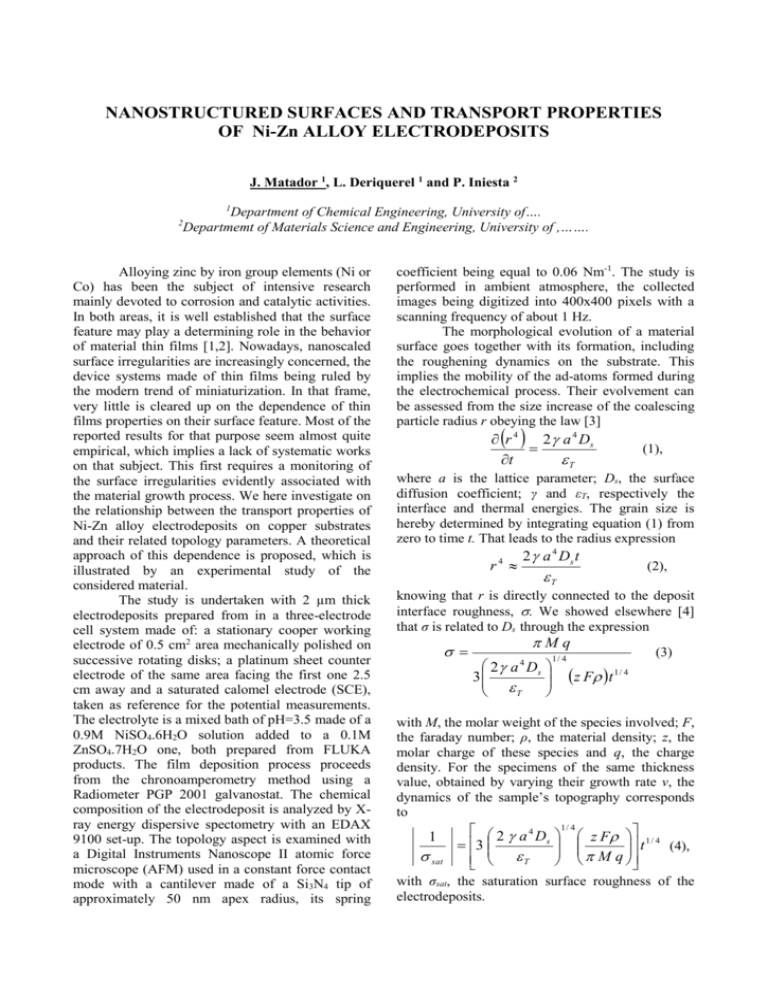
NANOSTRUCTURED SURFACES AND TRANSPORT PROPERTIES OF Ni-Zn ALLOY ELECTRODEPOSITS J. Matador 1, L. Deriquerel 1 and P. Iniesta 2 Department of Chemical Engineering, University of…. Departmemt of Materials Science and Engineering, University of ,……. 1 2 Alloying zinc by iron group elements (Ni or Co) has been the subject of intensive research mainly devoted to corrosion and catalytic activities. In both areas, it is well established that the surface feature may play a determining role in the behavior of material thin films [1,2]. Nowadays, nanoscaled surface irregularities are increasingly concerned, the device systems made of thin films being ruled by the modern trend of miniaturization. In that frame, very little is cleared up on the dependence of thin films properties on their surface feature. Most of the reported results for that purpose seem almost quite empirical, which implies a lack of systematic works on that subject. This first requires a monitoring of the surface irregularities evidently associated with the material growth process. We here investigate on the relationship between the transport properties of Ni-Zn alloy electrodeposits on copper substrates and their related topology parameters. A theoretical approach of this dependence is proposed, which is illustrated by an experimental study of the considered material. The study is undertaken with 2 µm thick electrodeposits prepared from in a three-electrode cell system made of: a stationary cooper working electrode of 0.5 cm2 area mechanically polished on successive rotating disks; a platinum sheet counter electrode of the same area facing the first one 2.5 cm away and a saturated calomel electrode (SCE), taken as reference for the potential measurements. The electrolyte is a mixed bath of pH=3.5 made of a 0.9M NiSO4.6H2O solution added to a 0.1M ZnSO4.7H2O one, both prepared from FLUKA products. The film deposition process proceeds from the chronoamperometry method using a Radiometer PGP 2001 galvanostat. The chemical composition of the electrodeposit is analyzed by Xray energy dispersive spectometry with an EDAX 9100 set-up. The topology aspect is examined with a Digital Instruments Nanoscope II atomic force microscope (AFM) used in a constant force contact mode with a cantilever made of a Si3N4 tip of approximately 50 nm apex radius, its spring coefficient being equal to 0.06 Nm-1. The study is performed in ambient atmosphere, the collected images being digitized into 400x400 pixels with a scanning frequency of about 1 Hz. The morphological evolution of a material surface goes together with its formation, including the roughening dynamics on the substrate. This implies the mobility of the ad-atoms formed during the electrochemical process. Their evolvement can be assessed from the size increase of the coalescing particle radius r obeying the law [3] 2 a 4 Ds r4 t T (1), where a is the lattice parameter; Ds, the surface diffusion coefficient; γ and εT, respectively the interface and thermal energies. The grain size is hereby determined by integrating equation (1) from zero to time t. That leads to the radius expression r4 2 a 4 Ds t (2), T knowing that r is directly connected to the deposit interface roughness, . We showed elsewhere [4] that σ is related to Ds through the expression Mq 2 a Ds 3 T 4 1/ 4 (3) z F t 1/ 4 with M, the molar weight of the species involved; F, the faraday number; ρ, the material density; z, the molar charge of these species and q, the charge density. For the specimens of the same thickness value, obtained by varying their growth rate v, the dynamics of the sample’s topography corresponds to 1 sat 2 a4D s 3 T 1/ 4 z F 1 / 4 t (4), M q with σsat, the saturation surface roughness of the electrodeposits. This topology parameter is determined by the family-Vicsek approach [5] from the sample’s AFM images, following the scaling behavior of the local interface roughness (nm) against the scan length, L (nm). One sees in Fig. 1 that sat ≈ 44 nm is here reached for the growth rate value v = 0.36 µm/s. We showed that the dependence of σsat on v value is non monotonous within our v investigation region. Fig.3 evidences three growth regimes of the ad-atoms formed on the copper substrate. The film thickness being constant, the variation of v implies the one of the deposition time, t, since both parameters are each other inversely proportional. 1.8 80 Saturation roughness, sat (nm) Surface roughness, log[ (nm)] 1.6 1.4 1.2 0.83 ± 0.02 1 0.8 L 60 40 Lc 20 0.6 1.5 2 2.5 3 3.5 4 Scan length, log[L (nm)] 4.5 5 5.5 Fig.1 - Evolution of the local interface roughness versus scan length A variety of surface features is obtained in respect to the growth rate, v(µm/s). This suggests a possible monitoring of the electrodeposit topography, which is of great interest for specific application fields. nm a) 0 0,1 Growth 1 nm nm b) nm Fig. 2 – AFM images of Ni-Zn deposits obtained at: v = 0.12 µm/s (a) and v = 0.05 µm/s (b) The surface of Fig. 2(a) exhibits a wide active area [6] relevant for catalytic investigations while the one of Fig. 2(b) depicts a lower active area suitable for corrosion resistance studies 0,4 0,5 The drawing of experimental σsat versus t curves for each of the regimes allows the determination of the related material diffusion coefficient (Ds) and length () as reported below. Regime nm 0,3 Fig.3 - Dependence of the saturation roughness versus the electrodeposit growth rate. regimes nm 0,2 Growth velocity, v (µm/s) v (cm /s) (µm) v < 0.17 1.76x10⁻¹⁰ 0.85 2.10x10⁻¹⁰ 0.45 2.40x10⁻⁸ 3.47 0.17 <v < 2 0.35 3 2 (µm/s) Regime Regime Ds v > 0.35 References [1] N. R. Short, A. Abibsi, J. K. Dennis, Trans. Inst. Metal Finish, Vol. 67, Pages 73- (1989) [2] K. Lohrberg, P. Kohl, Electrochim. Acta, Vol. 29, Pages 2557- (1984) [3] C. Alonso, R. C. Salvarreza, J. M. Vara, A. J. Arvia, L. Vàzquez, A. Bartolome, A. M. Baro, J. Electrochem. Soc., Vol. 137, Pages 2161- (1990) [4] M. Hiane, J. Ebothé, Eur. Phys. J. B, Vol. 22, Pages 485-495 (2001). [5] F. Family, T. Vicsek, J. Phys. A, Vol. 18, Pages L75- (1985) [6] J. Ebothé, M. Hiane, Appl. Surf. Sci, Vol 183, Pages 93-102
