ECE 599-003 (NE-2) Fundamentals of Nanoscale Fabrication
advertisement
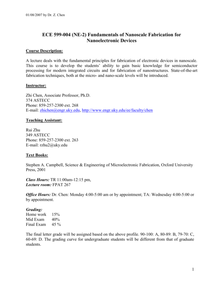
01/08/2007 by Dr. Z. Chen ECE 599-004 (NE-2) Fundamentals of Nanoscale Fabrication for Nanoelectronic Devices Course Description: A lecture deals with the fundamental principles for fabrication of electronic devices in nanoscale. This course is to develop the students’ ability to gain basic knowledge for semiconductor processing for modern integrated circuits and for fabrication of nanostructures. State-of-the-art fabrication techniques, both at the micro- and nano-scale levels will be introduced. Instructor: Zhi Chen, Associate Professor, Ph.D. 374 ASTECC Phone: 859-257-2300 ext. 268 E-mail: zhichen@engr.uky.edu, http://www.engr.uky.edu/ee/faculty/chen Teaching Assistant: Rui Zhu 349 ASTECC Phone: 859-257-2300 ext. 263 E-mail: rzhu2@uky.edu Text Books: Stephen A. Campbell, Science & Engineering of Microelectronic Fabrication, Oxford University Press, 2001 Class Hours: TR 11:00am-12:15 pm, Lecture room: FPAT 267 Office Hours: Dr. Chen: Monday 4:00-5:00 am or by appointment; TA: Wednesday 4:00-5:00 or by appointment. Grading: Home work Mid Exam Final Exam 15% 40% 45 % The final letter grade will be assigned based on the above profile. 90-100: A, 80-89: B, 79-70: C, 60-69: D. The grading curve for undergraduate students will be different from that of graduate students. 1 01/08/2007 by Dr. Z. Chen Course Topics: Introduction A. Overview of Microelectronics B. Semiconductor Wafers Hot processing and Ion Implantation A. Diffusion B. Thermal oxidation C. Ion implantation D. Rapid thermal processing Pattern transfer A. Optical lithography B. Photoresist C. Nonoptical lithography D. Vacuum science and technology E. Etching Thin Films A. Physical deposition B. Chemical vapor deposition C. Epitaxial growth Upon completion of this course students should demonstrate the abilities to: a. Understand the basic principle for optical, e-beam, and x-ray lithography b. Understand the basic principle for wet chemical etching and dry etching c. Understand the basic principle for ion implantation and be able to control range of implantation d. Understand the principle for thin film deposition and crystal growth using CVD and MBE. POLICIES: Homework policy: Homework will generally be assigned each week on Tuesday and due the following Tuesday. The homework is to be turned in at the beginning of the class period. No late homework will be accepted. Solutions to all homework problems will be given in class after the homework being turned in. Students finding difficulty understanding a particular topic or homework problem are encouraged to meet with the instructor during office hours. Exam policy: There will be a mid-term exam and a final exam. Failure to write an exam will result in a score of zero. No makeup exams will be given. Upon the receipt of a graded exam, if you find that an exam problem was graded incorrectly, it must be re-submitted to the instructor within 24 hours from the time the exam was returned. It will take about one hour for the midterm exam and two hours for the final exam. 2
