version - Brigham Young University
advertisement
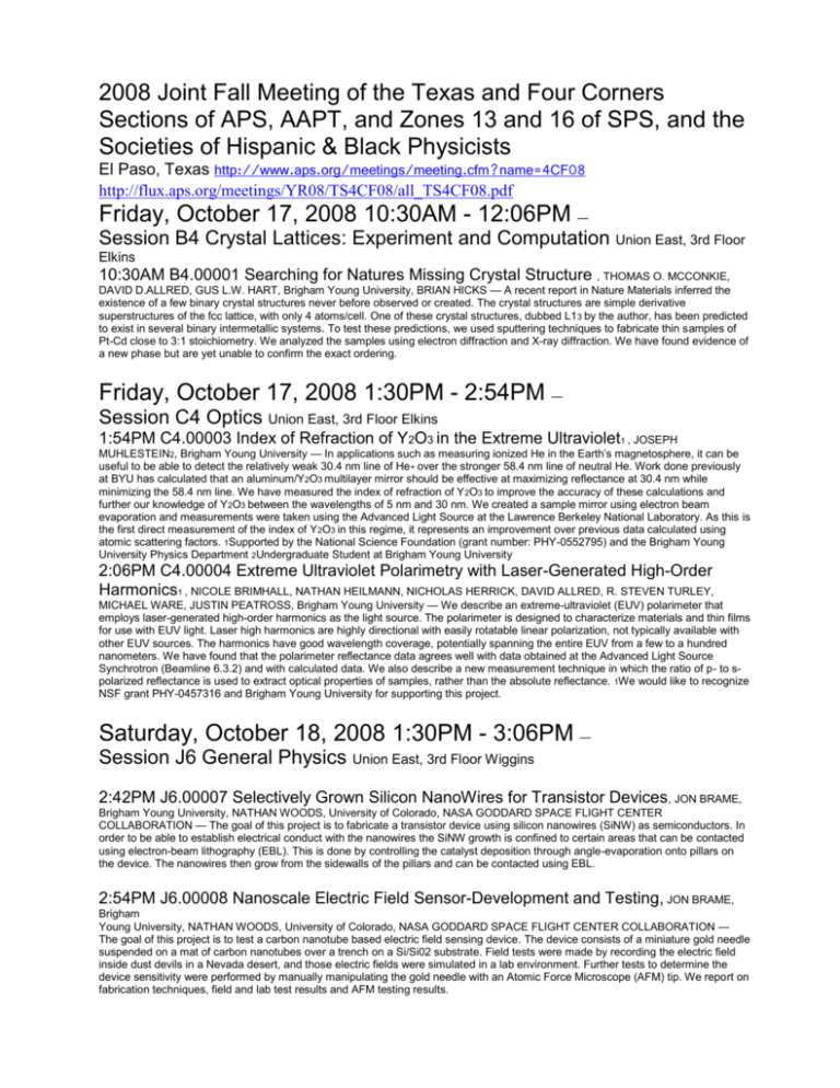
2008 Joint Fall Meeting of the Texas and Four Corners Sections of APS, AAPT, and Zones 13 and 16 of SPS, and the Societies of Hispanic & Black Physicists El Paso, Texas http://www.aps.org/meetings/meeting.cfm?name=4CF08 http://flux.aps.org/meetings/YR08/TS4CF08/all_TS4CF08.pdf Friday, October 17, 2008 10:30AM - 12:06PM — Session B4 Crystal Lattices: Experiment and Computation Union East, 3rd Floor Elkins 10:30AM B4.00001 Searching for Natures Missing Crystal Structure , THOMAS O. MCCONKIE, DAVID D.ALLRED, GUS L.W. HART, Brigham Young University, BRIAN HICKS — A recent report in Nature Materials inferred the existence of a few binary crystal structures never before observed or created. The crystal structures are simple derivative superstructures of the fcc lattice, with only 4 atoms/cell. One of these crystal structures, dubbed L1 3 by the author, has been predicted to exist in several binary intermetallic systems. To test these predictions, we used sputtering techniques to fabricate thin samples of Pt-Cd close to 3:1 stoichiometry. We analyzed the samples using electron diffraction and X-ray diffraction. We have found evidence of a new phase but are yet unable to confirm the exact ordering. Friday, October 17, 2008 1:30PM - 2:54PM — Session C4 Optics Union East, 3rd Floor Elkins 1:54PM C4.00003 Index of Refraction of Y2O3 in the Extreme Ultraviolet1 , JOSEPH MUHLESTEIN2, Brigham Young University — In applications such as measuring ionized He in the Earth’s magnetosphere, it can be useful to be able to detect the relatively weak 30.4 nm line of He+ over the stronger 58.4 nm line of neutral He. Work done previously at BYU has calculated that an aluminum/Y2O3 multilayer mirror should be effective at maximizing reflectance at 30.4 nm while minimizing the 58.4 nm line. We have measured the index of refraction of Y 2O3 to improve the accuracy of these calculations and further our knowledge of Y2O3 between the wavelengths of 5 nm and 30 nm. We created a sample mirror using electron beam evaporation and measurements were taken using the Advanced Light Source at the Lawrence Berkeley National Laboratory. As this is the first direct measurement of the index of Y2O3 in this regime, it represents an improvement over previous data calculated using atomic scattering factors. 1Supported by the National Science Foundation (grant number: PHY-0552795) and the Brigham Young University Physics Department 2Undergraduate Student at Brigham Young University 2:06PM C4.00004 Extreme Ultraviolet Polarimetry with Laser-Generated High-Order Harmonics1 , NICOLE BRIMHALL, NATHAN HEILMANN, NICHOLAS HERRICK, DAVID ALLRED, R. STEVEN TURLEY, MICHAEL WARE, JUSTIN PEATROSS, Brigham Young University — We describe an extreme-ultraviolet (EUV) polarimeter that employs laser-generated high-order harmonics as the light source. The polarimeter is designed to characterize materials and thin films for use with EUV light. Laser high harmonics are highly directional with easily rotatable linear polarization, not typically available with other EUV sources. The harmonics have good wavelength coverage, potentially spanning the entire EUV from a few to a hundred nanometers. We have found that the polarimeter reflectance data agrees well with data obtained at the Advanced Light Source Synchrotron (Beamline 6.3.2) and with calculated data. We also describe a new measurement technique in which the ratio of p- to spolarized reflectance is used to extract optical properties of samples, rather than the absolute reflectance. 1We would like to recognize NSF grant PHY-0457316 and Brigham Young University for supporting this project. Saturday, October 18, 2008 1:30PM - 3:06PM — Session J6 General Physics Union East, 3rd Floor Wiggins 2:42PM J6.00007 Selectively Grown Silicon NanoWires for Transistor Devices , JON BRAME, Brigham Young University, NATHAN WOODS, University of Colorado, NASA GODDARD SPACE FLIGHT CENTER COLLABORATION — The goal of this project is to fabricate a transistor device using silicon nanowires (SiNW) as semiconductors. In order to be able to establish electrical conduct with the nanowires the SiNW growth is confined to certain areas that can be contacted using electron-beam lithography (EBL). This is done by controlling the catalyst deposition through angle-evaporation onto pillars on the device. The nanowires then grow from the sidewalls of the pillars and can be contacted using EBL. 2:54PM J6.00008 Nanoscale Electric Field Sensor-Development and Testing, JON BRAME, Brigham Young University, NATHAN WOODS, University of Colorado, NASA GODDARD SPACE FLIGHT CENTER COLLABORATION — The goal of this project is to test a carbon nanotube based electric field sensing device. The device consists of a miniature gold needle suspended on a mat of carbon nanotubes over a trench on a Si/Si02 substrate. Field tests were made by recording the electric field inside dust devils in a Nevada desert, and those electric fields were simulated in a lab environment. Further tests to determine the device sensitivity were performed by manually manipulating the gold needle with an Atomic Force Microscope (AFM) tip. We report on fabrication techniques, field and lab test results and AFM testing results.
