Deney4
advertisement
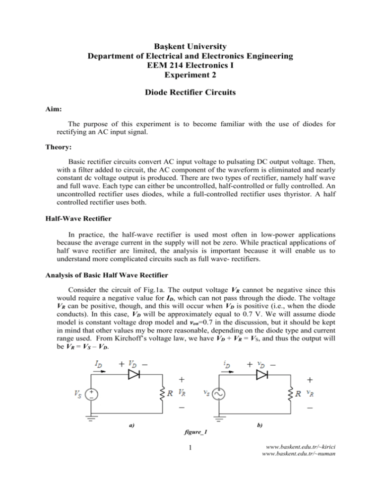
Başkent University Department of Electrical and Electronics Engineering EEM 214 Electronics I Experiment 2 Diode Rectifier Circuits Aim: The purpose of this experiment is to become familiar with the use of diodes for rectifying an AC input signal. Theory: Basic rectifier circuits convert AC input voltage to pulsating DC output voltage. Then, with a filter added to circuit, the AC component of the waveform is eliminated and nearly constant dc voltage output is produced. There are two types of rectifier, namely half wave and full wave. Each type can either be uncontrolled, half-controlled or fully controlled. An uncontrolled rectifier uses diodes, while a full-controlled rectifier uses thyristor. A half controlled rectifier uses both. Half-Wave Rectifier In practice, the half-wave rectifier is used most often in low-power applications because the average current in the supply will not be zero. While practical applications of half wave rectifier are limited, the analysis is important because it will enable us to understand more complicated circuits such as full wave- rectifiers. Analysis of Basic Half Wave Rectifier Consider the circuit of Fig.1a. The output voltage VR cannot be negative since this would require a negative value for ID, which can not pass through the diode. The voltage VR can be positive, though, and this will occur when VD is positive (i.e., when the diode conducts). In this case, VD will be approximately equal to 0.7 V. We will assume diode model is constant voltage drop model and von=0.7 in the discussion, but it should be kept in mind that other values my be more reasonable, depending on the diode type and current range used. From Kirchoff’s voltage law, we have VD + VR = VS, and thus the output will be VR = VS – VD. a) b) figure_1 1 www.baskent.edu.tr/~kirici www.baskent.edu.tr/~numan Assume now that vS is a sinusoidal voltage as shown in Fig.1b. From the above observations, it can be seen that the output voltage waveform vR is as shown in Fig. 2. The negative parts of each input cycle are cut off, since vR cannot be negative. During conduction the positive parts of each input cycle appear at the output, but are lowered by the voltage of the forward-biased diode (assumed to be about 0.7 V in the figure). The circuit in Fig.1b is called a basic half wave rectifier. Figure_2 The output voltage v in Fig. 2 has only one polarity, in contrast to the input voltage. However, it is not a DC voltage, as it is not constant with time. We can obtain a voltage that is almost DC by adding a capacitor to the circuit, as shown in Fig.3a. This results in the behavior shown in Fig. 3b, as will now be explained. When the diode conducts, vR = vS – vD, and the capacitor charges up to this value. Let the peak value of the input voltage be vP. Near the peaks of the input voltage, the capacitor voltage is approximately vR = vP – 0.7 V. When vS decreases below its peak value, the value of vD = vS – vR decreases since vR is held almost constant by the capacitor. Thus the diode becomes cut off, and its current reduces practically to zero; it now behaves virtually as an open circuit. The capacitor is then effectively connected only to the resistor and begins discharging through it. If the RC time constant is large, the discharge will be slow, as shown in Fig.3b. At some later point, the input rises again and reaches a value about 0.7V higher than the value of vR; then the diode starts conducting again, and vR = vS – vD ≈ vS – 0.7V. The output thus starts following the rising input (while staying below it by about 0.7 V). The capacitor charges up again, and the whole cycle is repeated. It can be seen that, for the circuit of Fig.3a, the output voltage is almost DC; it is constant within a small variation, called the ripple. The ripple can be made very small by choosing an appropriate RC time constant. a) b) figure_3 2 www.baskent.edu.tr/~kirici www.baskent.edu.tr/~numan Full-Wave Rectifier Like half-wave, the objective of a full-wave rectifier is to produce a voltage or current which is purely DC or has some specified dc component. While the purpose of the fullwave rectifier is basically the same as that of the half-wave rectifiers, full wave rectifier has some fundamental advantages. The average current in the ac source is zero in the fullwave rectifier, thus avoiding problems associated with nonzero average source currents. The average (dc) output voltage is higher than half-wave. The output of the full-wave has inherently less ripple that the half-wave rectifier. The Average and RMS values of Signal T Vavg VDC T 1 V (t )dt T0 Vrms 1 (V (t )) 2 dt T0 V(t) : Signal T : Period of signal 3 www.baskent.edu.tr/~kirici www.baskent.edu.tr/~numan Preliminary Work: 1) Review the sections 3.13,.3.14, 3.15,3.16 from text book. 2) a. For the half wave rectifier circuit in Fig.4a, draw the input and output voltage waveforms (explain briefly how you obtain), assume diode model is constant voltage drop, vi(t)=5sin(200πt) and RL=1k. Construct and simulate the circuit using PSPICE and get the waveform of the output and input voltage at same plot and get the waveform of diode current in different plot also obtain DC(average) and RMS values of the output voltage using PSPICE add trace button. Check your drawing with the simulation. figure_4 b. For the half wave rectifier circuit with capacitive load in Fig.4b, draw the waveform of the input and output voltage (explain briefly how you obtain), assume diode model is constant voltage drop, vi(t)=5sin(200πt), C=10μF and RL=1k. Find the PIV ratings of diodes. Construct and simulate the circuit using PSPICE and get the waveform of the input and output voltage at same plot and diode current in different plot also obtain DC(average) value of the output voltage using PSPICE add trace button. Check your drawing with the simulation. c. Compare the circuit of Fig.4a and Fig.4b according to diode currents and DC values of the output voltages. 3) a. For the full wave bridge rectifier circuit in Fig..5a, draw the waveform of the input and output voltage (explain briefly how you obtain), assume diode model is constant voltage drop, vi(t)=5sin(200πt) and RL=1k. Calculate the DC(average) and RMS values of the output signal. Construct and simulate the circuit using PSPICE and get the waveform of the input and output voltage at same plot and get the diode current in different plots also obtain DC(average) and RMS values of the output voltage using PSPICE add trace button. Check your drawing with the simulation. 4 www.baskent.edu.tr/~kirici www.baskent.edu.tr/~numan b. For the full wave bridge rectifier circuit with capacitive load in Fig.5b, draw the waveform of the input and output voltage (explain briefly how you obtain), assume diode model is constant voltage drop, vi(t)=5sin(200πt), C=10μF and RL=1k. Find the PIV ratings of diodes. Construct and simulate the circuit using PSPICE and get the waveform of the input and output voltage at same plot and get diode current in different plot also obtain DC(average) value of the output voltage using PSPICE add trace button. Check your drawing with the simulation. figure_5 4) Compare the circuit of Fig.4b and Fig.5b according to PIV Ratings Diode currents Complexity of circuits 5) Design Problem: Consider the full wave bridge rectifier circuit with capacitive load in Fig.4b, assume diode model is constant voltage drop, vi(t)=5sin(200πt) and C=100μF. It is desired that the peak to peak ripple voltage Vr to be less than 1% of the input voltage. Determine the value of RL and draw output voltage. Show all your calculations and assumptions. 5 www.baskent.edu.tr/~kirici www.baskent.edu.tr/~numan Construct and simulate the circuit using PSPICE and obtain the waveform of the output voltage also obtain DC(average) value of the output voltage. Measure the peak to peak ripple and check whether your design is correct or not. 6) Read the experiment. Experimental Work: 220 V AC 6 - 30V AC figure_6 a) 220 V AC 6 - 30V AC VOUT figure_6 b) 6 www.baskent.edu.tr/~kirici www.baskent.edu.tr/~numan 1) a. Setup the circuit of Fig.4a. Set the input voltage signal (with transformer box) to 6V amplitude with RL=1k. Obtain and plot the input and output voltage waveforms; compare the peak values of the input and the output. Measure the DC value of the output voltage. vin & vout vout-DC = b. Setup the circuit in Fig.4b which has capacitive load other than circuit in Fig.4b. Set the input voltage signal (with transformer box) to 6V amplitude with C=10μF and RL=1k. Obtain and plot the input and output voltage waveforms; compare the peak values of the input and the output. Measure the DC value of the output voltage. Obtain the frequency of the “ripple voltage” across the load resistor and measure the peak to peak ripple voltage. Also try the cases with C=1μF. Comment on result. 7 www.baskent.edu.tr/~kirici www.baskent.edu.tr/~numan vin & vout (C =10μF) vin & vout (C =1μF) C =10μF C =1μF vout-DC 8 www.baskent.edu.tr/~kirici www.baskent.edu.tr/~numan f ripple vpeaktopeak-ripple 2) a. Setup the circuit of Fig.6a. Set the input voltage signal (with transformer box) to 6V amplitude with RL=1k. Obtain and plot the input and output voltage waveforms; compare the peak values of the input and the output. Measure the DC value of the output voltage. vin & vout vout-DC = b. Setup the circuit in fig.6b which has capacitive load other than circuit in Fig.6a. Set the input voltage signal (with transformer box) to 6V amplitude with C=10μF and RL=1k. Obtain the input and output voltage waveforms; compare the peak values of the input and the output. Measure the DC value of the output voltage. Obtain the frequency of the “ripple voltage” across the load resistor and measure the peak to peak ripple voltage. Also try the cases with C=1μF. Comment on result. 9 www.baskent.edu.tr/~kirici www.baskent.edu.tr/~numan vin & vout (C =10μF) vin & vout (C =1μF) 10 www.baskent.edu.tr/~kirici www.baskent.edu.tr/~numan C =10μF C =1μF vout-DC f ripple vpeaktopeak-ripple 3) In half or a full wave rectifier with capacitive load, how can you improve the ripple if the output resistance is constant? 4) Setup the circuit of Fig.6, Set the input voltage signal (with transformer box) to 15V amplitude with C=22μF, R=330, RL= 1k. a. Disconnect the zener diode. Obtain and plot input and output voltages. Measure and record the DC value of the output voltage and peak to peak ripple voltage. Comment on result. vin & vout vout-DC = vpeaktopeak-ripple = 11 www.baskent.edu.tr/~kirici www.baskent.edu.tr/~numan b. Connect the zener diode. Obtain and plot input and output voltages. Measure and record DC value of the output voltage and peak to peak ripple voltage. Comment on the results. vin & vout vout-DC = vpeaktopeak-ripple = c. Briefly explain what is the circuit used for? 12 www.baskent.edu.tr/~kirici www.baskent.edu.tr/~numan 220 V AC 6 - 30V AC VOUT figure_6 Lab Instruments: Breadboard Oscilloscope Signal Generator Multimeter Components: 4 1N4148 1 1N748 1 10μF 1 22μF 1 1 1 1μF 330 1k ...............................……………………………………………………………….. Experiment Results a. vout-DC = Part1 C =10μF b. C =1μF vout-DC f ripple 13 www.baskent.edu.tr/~kirici www.baskent.edu.tr/~numan vpeaktopeak-ripple a. vout-DC = C =10μF Part2 b. C =1μF vout-DC f ripple vpeaktopeak-ripple a. vout-DC = vpeaktopeak-ripple = b. vout-DC = vpeaktopeak-ripple = Part4 Student Name : Number : Signature…………….…………. 14 www.baskent.edu.tr/~kirici www.baskent.edu.tr/~numan
