First Performance Results from a Real Size Silicon Pad Sensor
advertisement
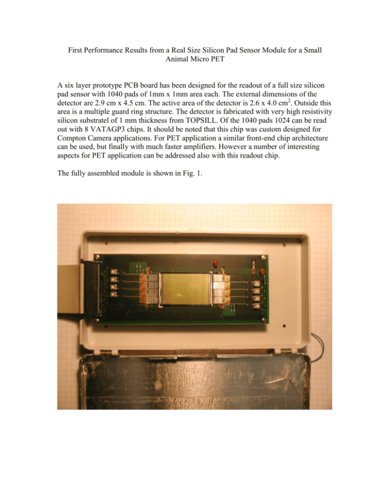
First Performance Results from a Real Size Silicon Pad Sensor Module for a Small Animal Micro PET A six layer prototype PCB board has been designed for the readout of a full size silicon pad sensor with 1040 pads of 1mm x 1mm area each. The external dimensions of the detector are 2.9 cm x 4.5 cm. The active area of the detector is 2.6 x 4.0 cm2. Outside this area is a multiple guard ring structure. The detector is fabricated with very high resistivity silicon substratel of 1 mm thickness from TOPSILL. Of the 1040 pads 1024 can be read out with 8 VATAGP3 chips. It should be noted that this chip was custom designed for Compton Camera applications. For PET application a similar front-end chip architecture can be used, but finally with much faster amplifiers. However a number of interesting aspects for PET application can be addressed also with this readout chip. The fully assembled module is shown in Fig. 1. Fig 1 Fully assembled PET prototype module Fig 1a Fig 2: Bond connections between Detector and chip, on detector side Fig. 3 Routing lines on second metal level from p+ pads to bond pads Fig 2 show a micrograph of bond connections from detector to chip Fig. 3 demonstrates the double metal technology with routing of sensor pads to the periphery of the detector to allow for conventional wire bonding to readout chips. The pad detector has an average leakage current in one pad of about 400 pA above the full depletion voltage of 150 V. The capacitive load of one pad is dominated by the routing lines and is estimated to be around 5 pF. Due to the particular layout of the routing lines the capacitance of all pads is nearly identical. Some data were taken with different and X-ray sources. Fig 4 shows the hit map of the module illuminated with the 57Co source. The source was positioned in the middle of the detector with respect to the bond pad rows and the long sides. The hit distribution in Fig 2 shows the regular pattern of 20 pads in each of the 26 pad columns being routed to the edge. Fig. 4 Hit map on detector with 57Co source Fig. 5 shows the total spectrum ( energy in ADC counts) in one channel obtained with the 57Co source. The data are taken in sparse readout mode. Serial readout mode gives very similar results The lines at 122 keV and 136 keV are at ~300 and ~330 ADC counts. At about 75 ADC counts ( corresponding to ~50 keV) the Compton edge, resulting from the signals of the Compton recoil electrons in the silicon, rises very steeply and extends to about 25 keV. The cut-off here is due to a relatively high threshold setting for the VATAGP3 chips. The lowest possible threshold with this module is around 14 keV. The lower cutoff near 0 ADC counts is an artifact of a pedestal shift in this readout mode. Fig 6 is a fit to the 122keV peak giving a sigma of ~2.5 ADC counts equivalent to a noise of 240 e- ENC. Fig. 5 The 57Co spectrum Fig. 6 Gaussian fit to 122 keV line This test proves that a full size PET pad detector of 1 mm thickness can be operated with self-triggering front-end chips. A second module will be built to demonstrate in a test setup with two detectors that the spatial resolution in PET mode of 500 micron FWHM in the image plane can be achieved. For further Compton PET prototype studies a very fast readout chip based on a similar architecture as the VATAGP3 chip will be required. Also the technology for very dense packaging of detectors needs to be developed further.


