docx - digsys.upc.edu
advertisement
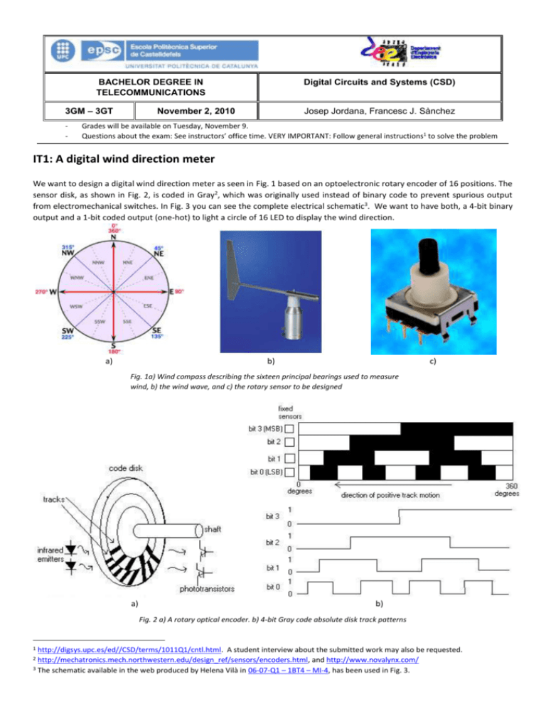
BACHELOR DEGREE IN TELECOMMUNICATIONS 3GM – 3GT - Digital Circuits and Systems (CSD) November 2, 2010 Josep Jordana, Francesc J. Sànchez Grades will be available on Tuesday, November 9. Questions about the exam: See instructors’ office time. VERY IMPORTANT: Follow general instructions1 to solve the problem IT1: A digital wind direction meter We want to design a digital wind direction meter as seen in Fig. 1 based on an optoelectronic rotary encoder of 16 positions. The sensor disk, as shown in Fig. 2, is coded in Gray2, which was originally used instead of binary code to prevent spurious output from electromechanical switches. In Fig. 3 you can see the complete electrical schematic3. We want to have both, a 4-bit binary output and a 1-bit coded output (one-hot) to light a circle of 16 LED to display the wind direction. a) b) c) Fig. 1a) Wind compass describing the sixteen principal bearings used to measure wind, b) the wind wave, and c) the rotary sensor to be designed a) b) Fig. 2 a) A rotary optical encoder. b) 4-bit Gray code absolute disk track patterns 1 http://digsys.upc.es/ed//CSD/terms/1011Q1/cntl.html. A student interview about the submitted work may also be requested. http://mechatronics.mech.northwestern.edu/design_ref/sensors/encoders.html, and http://www.novalynx.com/ 3 The schematic available in the web produced by Helena Vilà in 06-07-Q1 – 1BT4 – MI-4, has been used in Fig. 3. 2 Fig. 3 Electrical schematic. The picture it’s showing Gray code “0110”, which is “0100” in binary and corresponds to the wind direction “Est” 1. Write the truth table for each block. 2. Write each output as an equation of a sum of minterms or a product of maxterms 3. For the Gray to binary converter, draw the circuit using logic gates of its output B2 = f(X3, X2, X1, X0). 4. For the DEC 4:16, draw the circuit using logic gates of its output Y7_L = f( E, X3, X2, X1, X0). 5. Write the VHDL code for the Gray to binary using a behavioural style (not all, but a portion sufficient to show how the VHDL code will be organised). 6. Write the VHDL code for the DEC 4:16 using a structural style (gates) (not all the code but a portion sufficient to show how the VHDL code will be organised). Extra: Implement the project in ModelSim or Active-HDL and synthesise the circuit into a CPLD or FPGA. IT2: A 3-bit Gray up-down counter The aim is to build a 3-bit Gray code up and down synchronous counter with count enable and terminal count signals. The entity to be designed and its function table, is represented in Fig. 4. CE and UD_L are synchronous signals, thus, if they are active, the system only responds following a rising edge from the CLK signal. CD is the asynchronous clear direct, thus, every time it is active, the system immediately reset the outputs: Q(2..0) = “000”. TC8 is the terminal count: TC8 = ‘1’ when UP counting and Q(2..0) = “100” (the higher Gray code), and also TC8 = ‘1’ when DOWN counting and Q(2..0) = “000” ((the lower Gray code). CE UD_L CD CLK 3-bit Gray revertible synchronous counter Q2 Q1 TC8 CE 0 1 1 UD_L 1 0 Operating mode Do nothing (inhibit) Up Gray counting Down Gray counting Q0 Fig. 4 Entity for the counter and function table Planning 1. Write the Gray code for 3 bits. 2. Draw the state diagrams for the block following the indications specified in the function table. Name conveniently all the states. 3. Draw the timing diagram for the outputs of the system using the supplied sheet of paper where some input activity has been sketched. (see Developing 4. Draw the internal architecture of the FSM of 3 blocks and indicate where all the signals are going to be connected. 5. If the internal states are going to be coded in Gray: ATTRIBUTE syn_encoding OF State_type : TYPE IS "gray"; how many bits will be necessary for the present and future state signals? How many D-FF will use the state register? 6. Or instead, if the internal states are going to be coded in “one-hot”: ATTRIBUTE syn_encoding OF State_type : TYPE IS "one-hot"; how many bits will be necessary for the present and future state signals? How many D-FF will use the state register? 7. Write the ASM chart for the CC1 block (not all, but a portion sufficient to show how the VHDL code will be organised). Write a sample of its VHDL code. 8. Write the ASM chart for the CC2 block (not all, but a portion sufficient to show how the VHDL code will be organised). Write a sample of its VHDL code. Simulating 9. Write a sample of a TCL macro using the waveforms from the timing diagram. Suppose that TCLK = 1 kHz. Extra: Implement the project in ModelSim or Active-HDL and synthesise the circuit into a CPLD or FPGA. Name: Cooperative group: Fig. 5 Sample waveforms to demonstrate how the system works. Comments on the waveforms:
